


The short answer: PPA optimisation in physical design balances power, performance and area. Leakage is reduced with high-Vt cells on non-critical paths and power gating; dynamic power with clock gating, compact clock trees and short high-activity nets; area by downsizing cells with spare slack and removing unneeded buffers. Low-power designs also implement multiple voltage domains and power-gated regions from the UPF: voltage areas, level shifters, isolation and retention cells, power switches and separate power grids.
Timing gets most of the attention, but for phones, IoT devices and AI accelerators, power is often the harder target. This post covers how the P&R flow optimises power and area, and how low-power architectures are built physically. It combines my older posts on power optimisation, area optimisation, multi-voltage design and PD for low-power devices. For the RTL side, see low-power design techniques.
- The knobs
- Leakage and dynamic power in P&R
- Area recovery
- Multiple voltage domains
- Power gating in PD
- Measuring PPA
Table of Contents
Part 1: The knobs
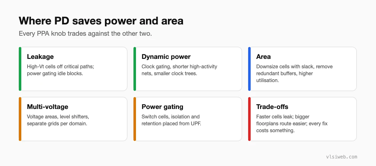
Part 2: Leakage and dynamic power in P&R
- Start optimisation with high-Vt or standard-Vt libraries and allow low-Vt only where timing needs it; report the Vt mix after each step.
- Optimise with switching activity (SAIF or VCD from simulation) so the tool shortens the nets that toggle most.
- Build the clock tree with power in mind: fewer levels, gating high in the tree, appropriate buffer sizes.
- Avoid over-fixing: every unnecessary upsized cell and buffer adds leakage and switching power.
Part 3: Area recovery
After timing is met, tools can recover area by downsizing cells on paths with positive slack and removing redundant buffers. Higher utilisation saves area too, but only if the design still routes and closes timing; I prefer to push utilisation once the floorplan is proven.
Part 4: Multiple voltage domains
- Each domain gets a voltage area in the floorplan and its own power grid.
- Level shifters are placed at domain crossings, usually at the boundary of the receiving domain.
- Timing uses libraries characterised at each domain’s voltage.
- Always-on cells inside switchable domains need their own supply routing.
Part 5: Power gating in PD
- Power switch cells are placed in a grid or ring across the switchable domain, sized for the current and the wake-up time.
- Switches are often daisy-chained to turn on gradually and limit rush current.
- Isolation cells sit on the outputs of the switchable domain; retention flops keep state on the always-on supply.
- Everything is driven by the UPF and checked by low-power static checks after placement and routing.
Part 6: Measuring PPA
| Metric | Where it comes from |
|---|---|
| Performance | Sign-off STA: achieved frequency, WNS/TNS |
| Dynamic power | Power analysis with real activity and extracted parasitics |
| Leakage | Power analysis at the leakage corner |
| Area | Cell area, utilisation and die size |
Track these per run. A good PD flow improves one without quietly giving away the others.
Practise this on VLSI Forge
I built VLSI Forge so you can write RTL in your browser, run it on a real simulator and check every signal in the waveform. Free, nothing to install.
Physical Design problems · Static Timing Analysis problems
Previous in my physical design series: Physical verification. Next: Tape-out and mask preparation.
FAQ
What is PPA in VLSI?
Power, performance and area: the three main metrics a design is optimised for, which usually trade against each other.
How does physical design reduce leakage?
By using high-Vt cells wherever timing allows and power-gating blocks that are idle.
What is a voltage area?
A region of the floorplan assigned to a power domain at a specific voltage, with its own power grid.
Why are power switches daisy-chained?
To turn the domain on gradually, limiting the rush current that could disturb the supply for neighbouring logic.
