

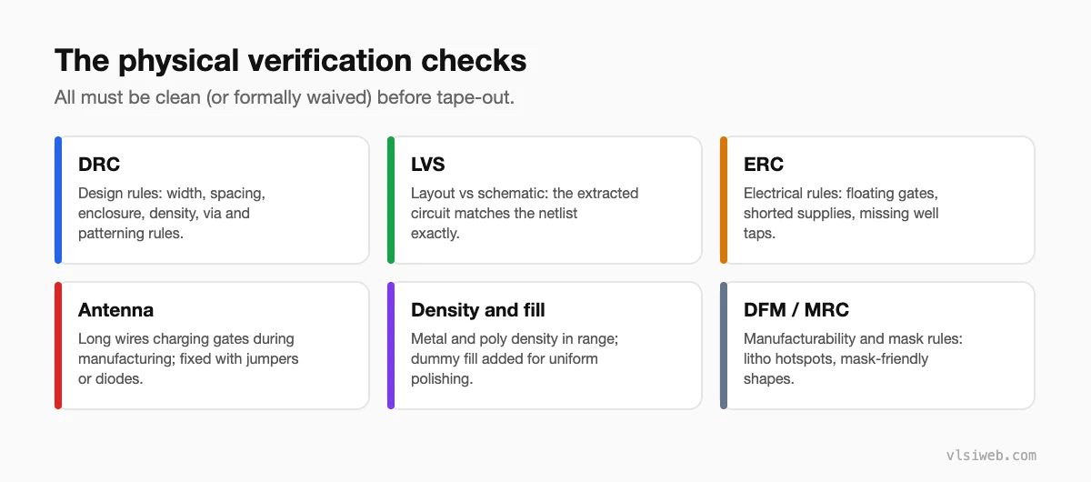
The short answer: Physical verification proves that the layout can be manufactured and matches the intended circuit. DRC checks the foundry’s geometric rules (widths, spacings, enclosures, density, patterning). LVS extracts the circuit from the layout and compares it with the netlist. ERC catches electrical problems such as floating gates or shorted supplies. Antenna checks protect gates from charge build-up during manufacturing, and density, fill, DFM and mask rule checks make the design manufacturable with good yield. Everything must be clean or formally waived before tape-out.
Timing and power can be perfect, but if the layout breaks one foundry rule or doesn’t match the netlist, the chip doesn’t get made, or doesn’t work. Physical verification is the final gate. This post combines my older posts on DRC, LVS, ERC, antenna effects and manufacturing rule checks.
- The checks
- DRC
- LVS
- ERC
- Antenna effect
- Density, fill and DFM
- How I run sign-off verification
Table of Contents
Part 1: The checks
Part 2: DRC
- Rules come from the foundry as a rule deck for the sign-off tool (Calibre, ICV, Pegasus).
- Basic rules: minimum width, spacing, area, enclosure of vias, notch and end-of-line rules.
- Advanced nodes add multiple patterning (colouring), fin and gate grid rules, and many via and cut rules.
- P&R tools check most rules during routing, but sign-off DRC with the official deck is the reference.
Part 3: LVS
LVS extracts devices and connectivity from the layout and compares them with the source netlist. Typical errors: shorts (two nets connected), opens (one net split), missing or extra devices, and wrong device sizes. Shorts between power and ground, or between signals in dense routing, are the most common at block level; mismatched pin names and missing labels are the most common at top level.
Part 4: ERC
Electrical rule checks find connections that are legal geometrically but wrong electrically: floating gate inputs, nets connected to both supplies, wells or substrate without proper ties, and incorrect connections across voltage domains (missing level shifters or isolation).
Part 5: Antenna effect
During manufacturing, long metal wires connected only to a transistor gate collect charge from the plasma etching steps, and the charge can damage the thin gate oxide. Antenna rules limit the ratio of metal area to gate area on each layer. Fixes:
- Layer jumping: break the long wire and continue it on a higher layer, so the gate isn’t connected until later steps.
- Antenna diodes near the gate to discharge the wire.
- Buffer insertion to split the net.
Part 6: Density, fill and DFM
Chemical-mechanical polishing needs metal and poly density within a range in every window, so tools add dummy fill in empty areas (and fill affects parasitics, so extraction is done with fill). DFM checks look for shapes that print poorly (litho hotspots) and recommend wider spacing or redundant vias to improve yield. Mask rule checks make sure the final shapes can be written on the masks.
Part 7: How I run sign-off verification
- Run DRC and LVS early on partial layouts so big problems surface before the end.
- Fix LVS before DRC: shorts often create many DRC errors.
- Keep a waiver list with reasons and approvals; never waive silently.
- Re-run everything after every ECO, however small.
Practise this on VLSI Forge
I built VLSI Forge so you can write RTL in your browser, run it on a real simulator and check every signal in the waveform. Free, nothing to install.
Previous in my physical design series: IR drop and electromigration. Next: PPA and low-power PD.
FAQ
What is the difference between DRC and LVS?
DRC checks that the layout obeys the foundry’s geometric rules; LVS checks that the layout’s circuit matches the netlist.
What is the antenna effect?
Charge collected on long metal wires during manufacturing that can damage the gate oxide of the transistors they connect to.
How do you fix antenna violations?
Layer jumping to a higher metal, adding antenna diodes, or buffering to shorten the wire connected to the gate.
What is metal fill?
Dummy metal shapes added to empty areas so metal density is uniform, which is required for chemical-mechanical polishing.
