

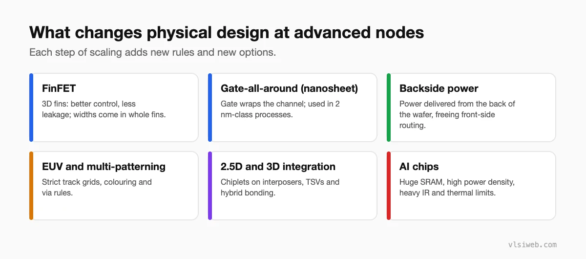
The short answer: At advanced nodes, transistors moved from planar to FinFET and now to gate-all-around nanosheets, wires got so thin that resistance and vias dominate delay, and lithography needs EUV and multiple patterning with strict routing grids. The newest processes add backside power delivery. At the same time, many designs are split into chiplets connected through 2.5D interposers or 3D stacking. For physical design, this means more rules, more variation, harder IR drop and thermal problems, and new floorplanning questions across dies.
Every node change shows up in the PD flow as new rules and new problems. This post is an overview of what changed from planar transistors to today’s processes and why it matters for implementation. It combines my older posts on advanced nodes, FinFET technology, 3D IC physical design and PD for AI chips.
- The big changes
- From planar to FinFET to GAA
- Wires are the bottleneck
- Lithography rules
- 2.5D and 3D integration
- Physical design for AI chips
Table of Contents
Part 1: The big changes
Part 2: From planar to FinFET to GAA
| Transistor | What changed | PD impact |
|---|---|---|
| Planar | Gate on top of a flat channel | Leakage grew quickly below about 28 nm |
| FinFET | Gate wraps three sides of a fin | Discrete widths (whole fins), fixed gate pitch, more pin-access rules |
| GAA / nanosheet | Gate surrounds stacked sheets | Better control and some width flexibility; new cell architectures |
Node names (7 nm, 5 nm, 3 nm, 2 nm) are marketing labels now; they don’t correspond to a physical gate length.
Part 3: Wires are the bottleneck
- Lower metal layers are so thin that their resistance rises sharply; long nets must use upper layers.
- Via resistance is significant, so via pillars and redundant vias are standard on critical nets.
- Electromigration limits are tighter, because wires carry similar currents in much smaller cross-sections.
- Backside power delivery moves the power grid under the transistors, reducing IR drop and freeing front-side tracks for signals.
Part 4: Lithography rules
EUV and multiple patterning bring fixed track patterns, colour assignment for shapes on the same layer, line-end and tip-to-tip rules, and cut-layer rules. Routers handle most of this automatically, but pin access and cell placement are much more constrained, and DRC decks are far larger than at older nodes.
Part 5: 2.5D and 3D integration
- Chiplets: large systems are split into smaller dies, possibly on different nodes, connected on a silicon interposer or bridge (2.5D). Smaller dies yield better.
- 3D stacking: dies stacked with through-silicon vias or hybrid bonding, giving very short vertical connections.
- PD impact: die-to-die interface planning, bump and TSV placement, thermal analysis across the stack, and multi-die timing and power sign-off.
Part 6: Physical design for AI chips
AI accelerators combine huge arrays of identical compute tiles with very large on-chip SRAM and high-bandwidth memory interfaces. Their PD challenges are high power density and dynamic IR drop (many MAC units switching together), thermal hotspots, floorplanning of memory-dominated layouts, and managing reuse of the same tile hundreds of times. Hierarchical flows and careful power grid design matter more than ever.
Practise this on VLSI Forge
I built VLSI Forge so you can write RTL in your browser, run it on a real simulator and check every signal in the waveform. Free, nothing to install.
Physical Design problems · Static Timing Analysis problems
Previous in my physical design series: Tape-out and mask preparation. Next: Tcl scripting for PD.
FAQ
What is a FinFET?
A transistor whose channel is a thin vertical fin with the gate wrapped around three sides, giving better control and lower leakage than planar transistors.
What is gate-all-around?
A transistor where the gate fully surrounds stacked nanosheet channels, used in 2 nm-class processes for even better control.
What is backside power delivery?
Routing the power network on the back of the wafer, under the transistors, which reduces IR drop and frees front-side metal for signals.
What is the difference between 2.5D and 3D ICs?
2.5D places dies side by side on an interposer; 3D stacks dies on top of each other, connected with TSVs or hybrid bonding.
