


The short answer: Chip power has two parts: dynamic power (roughly activity × capacitance × V² × frequency) and leakage. Clock gating and operand isolation cut activity; multi-voltage design and DVFS cut voltage and frequency; multi-Vt cells and power gating cut leakage. Power gating and multiple voltage domains need extra cells (isolation, retention, level shifters), which are described in a UPF power intent file and checked by the whole flow.
Power is now a first-class design goal, as important as timing and area, especially for mobile, IoT and AI chips. In this post I go through the main techniques, what each one saves, and what it costs in design and verification effort. It replaces my older post on low-power design.
- Where power goes
- Clock gating
- Multi-Vt cells
- Power gating
- Multiple voltages and DVFS
- Power intent: UPF
- Verifying low-power designs
Table of Contents
Part 1: Where power goes
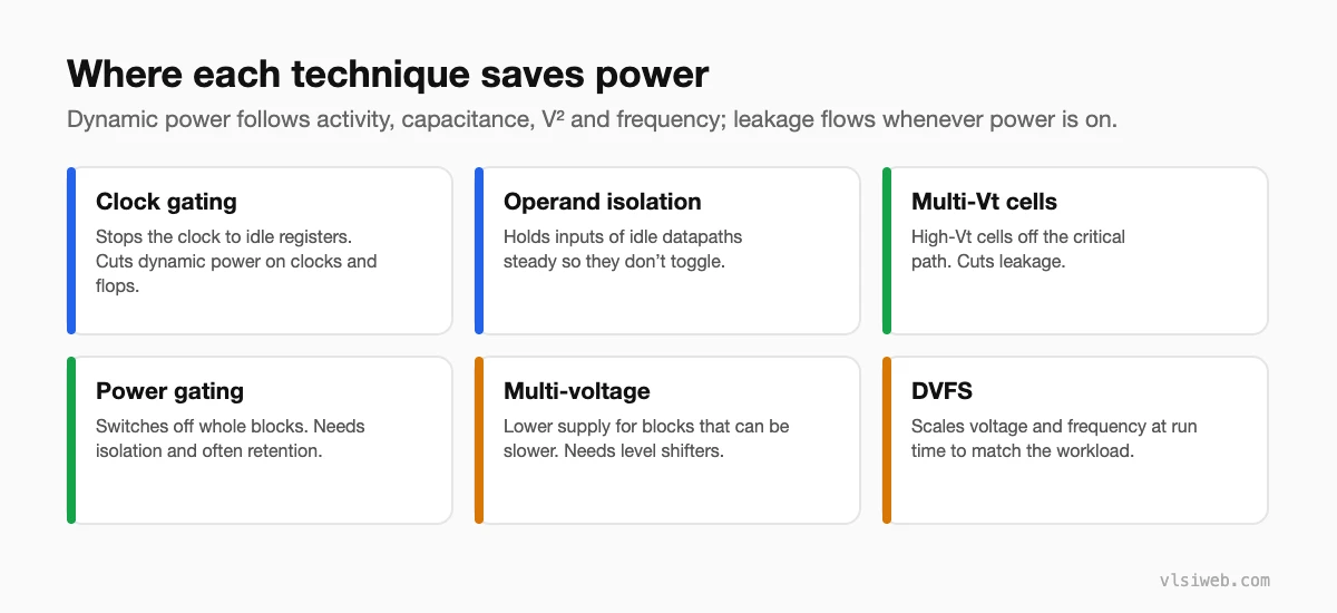
Because voltage appears squared in dynamic power, lowering the supply is the most powerful lever. The clock network alone is often a large share of dynamic power, which is why clock gating is everywhere.
Part 2: Clock gating
// RTL: just write the enable
always_ff @(posedge clk)
  if (en) data_q <= data_d;

// synthesis replaces the feedback mux with an integrated clock gating cell:
//   ICG: latch on enable + AND gate, so the gated clock can't glitch
Write enables in RTL and let synthesis insert ICG cells; don’t gate clocks with your own logic. For bigger savings, gate whole blocks with an architectural enable when they’re idle.
Part 3: Multi-Vt cells
Standard-cell libraries come in several threshold voltages. Low-Vt cells are fast but leak a lot; high-Vt cells are slower and leak much less. Tools start with high or standard Vt and swap to low Vt only on critical paths, often cutting leakage substantially with no timing loss.
Part 4: Power gating
- A header or footer switch disconnects a block’s supply when it isn’t needed, removing most of its leakage.
- Isolation cells clamp the outputs of an off block to a safe value, so powered-on logic doesn’t see floating signals.
- Retention registers keep key state on an always-on supply, so the block can resume quickly.
- A power controller sequences the steps: isolate, save, switch off; then switch on, restore, release isolation.
Part 5: Multiple voltages and DVFS
Blocks that don’t need full speed can run from a lower supply. Signals crossing between voltage domains need level shifters. Dynamic voltage and frequency scaling (DVFS) goes further, changing voltage and frequency at run time; the clock must be lowered before the voltage, and raised after it.
Part 6: Power intent: UPF
create_power_domain PD_CORE -elements {u_core}
create_supply_net    VDD_CORE
set_isolation  iso_core -domain PD_CORE -isolation_power_net VDD_AON \
               -clamp_value 0 -applies_to outputs
set_retention  ret_core -domain PD_CORE -retention_power_net VDD_AON
The Unified Power Format (IEEE 1801) describes domains, supplies, switches, isolation, retention and level shifters outside the RTL. Simulation, synthesis, place and route and sign-off all read the same UPF, so the RTL stays clean.
Part 7: Verifying low-power designs
- Run power-aware simulation, where signals in off domains go to x, to catch missing isolation.
- Test every power sequence: entry, exit, and events arriving during transitions.
- Use static low-power checks to find missing isolation or level shifters.
- Check that retention really restores state, and that resets behave correctly after power-up.
Practise this on VLSI Forge
I built VLSI Forge so you can write RTL in your browser, run it on a real simulator and check every signal in the waveform. Free, nothing to install.
FAQ
What is the formula for dynamic power?
Approximately P = α · C · V² · f, where α is switching activity, C the switched capacitance, V the supply voltage and f the clock frequency.
What is the difference between clock gating and power gating?
Clock gating stops the clock to save dynamic power but keeps the block powered. Power gating switches the supply off to save leakage, and needs isolation and retention.
What is UPF?
The Unified Power Format (IEEE 1801), a Tcl-based file that describes a design’s power domains, supplies and low-power cells separately from the RTL.
Why are level shifters needed?
Signals going between domains at different voltages may not switch the receiving logic correctly, so level shifters translate them to the right voltage.
