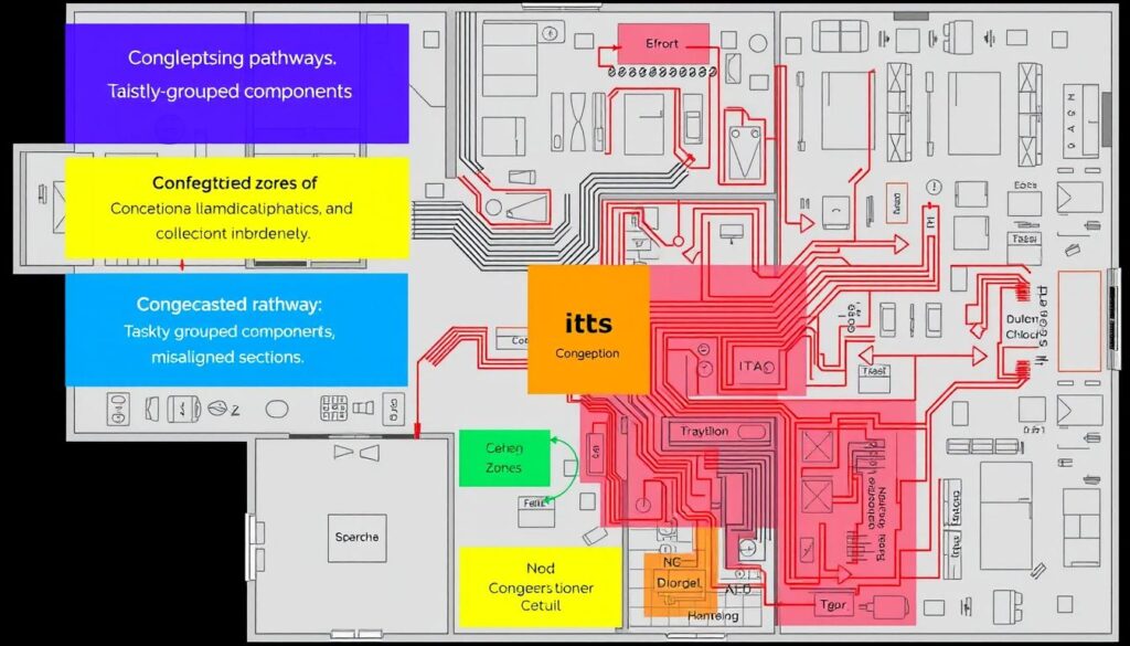
In the world of VLSI design, integrated circuits are key to modern tech. Managing circuit congestion is vital. During placement, congestion analysis is crucial for the circuit’s efficiency and reliability.
Congestion analysis checks if there’s enough room for wiring. PnR tools show problem areas as red “hotspots.” The area is split into squares called Global Routing Cells (GRCs) for this analysis.
Then, overflow is calculated to find out how congested it is. A GRC overflow under 1% is good for wiring. This ensures the circuit works well and meets standards.
Managing congestion well is essential for VLSI design success. It makes the circuit work smoothly. By tackling congestion early, designers can create top-notch technologies.
Table of Contents
Understanding VLSI Congestion and Its Impact
In the world of VLSI (Very Large-Scale Integration) chip design, congestion is a big deal. It affects how well and reliably the chip works. When there’s too much demand for routing tracks, it causes a lot of problems.
What Defines Congestion in VLSI Design
Congestion in VLSI design comes from many things. It’s about how packed the design is, the complexity of the paths, and how well the floorplan is done. It also depends on the design’s complexity and the resources available. All these can lead to congestion.
Impact on Chip Performance and Reliability
Congestion can really hurt a chip’s performance and reliability. It can slow down the chip, make wires longer, and increase resistance. This can lead to higher power use, manufacturing issues, and even heat problems.
Role of Global Routing Cells (GRC)
Global Routing Cells (GRCs) play a key role in understanding congestion. They break the design area into squares. Metrics like GRC overflow percentage help designers see how bad congestion is. Managing congestion well is key to meeting design goals like speed, power, and size.
| Congestion Metric | Description |
|---|---|
| GRC Overflow Percentage | Percentage of GRCs with routing demand exceeding capacity |
| Total Overflow | Sum of the overflows across all GRCs |
| Maximum Overflow per GRC | Highest overflow value observed in any individual GRC |
Understanding congestion in VLSI design is crucial. It helps designers find ways to improve the design process. This way, they can make chips that work better and last longer.
Primary Causes of Placement Congestion
Placement congestion in VLSI design comes from many factors. Each one needs careful analysis and specific fixes to boost chip performance and reliability. Knowing what causes placement congestion is key to tackling this big challenge.
Poor floorplanning and wrong macro placement are major culprits. If functional blocks aren’t placed wisely, it leads to routing problems. Also, too many standard cells in certain areas can block signal paths, causing congestion.
- Too many standard cells near macros: When lots of standard cells are near big macro blocks, it worsens congestion. This is because the demand for routes in these spots is too high.
- Routing blockages over standard cells: Barriers or limits on routing over standard cells can really cut down on available paths. This causes congestion and poor chip performance.
- High port density: Designs with lots of ports, mainly in certain spots, can block routes. This adds to overall placement congestion.
Also, not being able to reorder scan chains or mix/swapping them, and suboptimal netlist optimization, make congestion worse. These issues lead to a lack of routing resources. They must be tackled to ensure a successful chip.

By tackling these main causes of placement congestion, VLSI design teams can improve the chip’s physical layout. They can reduce routing bottlenecks. This leads to a high-performing and reliable chip design.
Congestion Analysis Methodologies and Tools
Congestion analysis is key in VLSI design. It helps find and fix high routing usage spots. PnR tools, like those for Placement and Routing, create detailed reports. These reports use different metrics and methods.
Global Routing Cell Analysis
Examining Global Routing Cells (GRCs) is a main way to analyze congestion. PnR tools break the chip into a grid of GRCs. They then check how full these areas are, showing congestion levels.
Overflow Calculation Methods
Tools calculate two important metrics for overflow: total and maximum overflow per GRC. Total overflow is the sum of all overflow routes. Maximum overflow per GRC shows the most congested spots. These help designers know where to focus on improving.
Tool-Specific Analysis Features
PnR tools have many features for congestion analysis. They use color-coded maps to show congested areas. Red spots highlight the worst congestion. Tools also offer detailed routing analysis and suggest ways to improve based on congestion patterns.
Managing congestion well is vital for high-performance VLSI designs. PnR tools help designers spot and fix congestion issues. This leads to better chip performance and less chance of design failures.
Advanced Congestion Alleviation Techniques
In VLSI design, fighting placement congestion needs a mix of strategies. Designers use advanced methods to spread cells, improve routing, and boost placement quality. By using placement blockages, cell padding, and power grid tweaks, congestion’s effects can be lessened.
Using partial or hard placement blockages is a smart move. These barriers help spread cells and open up routes. Also, keepout margins around macros keep cells apart, preventing overlap.
High-pin-count cells can cause congestion. Cell padding helps by giving these cells more space. This makes routing easier and reduces congestion. Power grid changes also help by improving routing resources.
Congestion-driven placement algorithms are key. They place cells to reduce congestion, making routing better. Incremental optimization further improves the design, reducing congestion’s impact.
By using these advanced techniques, designers can tackle placement challenges. These strategies improve design performance, reliability, and manufacturability.

| Technique | Description | Impact |
|---|---|---|
| Placement Blockages | Strategic use of partial or hard blockages to spread cells and restrict placement | Improves cell distribution and opens up routing channels |
| Keepout Margins | Implementation of halos around macros to maintain sufficient spacing | Prevents overlapping of nearby cells and enhances routing resources |
| Cell Padding | Allocation of additional space around high-pin-count cells | Improves routing resource utilization and reduces congestion |
| PG Grid Modification | Optimization of power grid layout to improve routing resource availability | Enhances the overall design’s performance and reliability |
| Congestion-Driven Placement | Algorithms that prioritize cell placement to minimize overall congestion | Optimizes the utilization of routing resources and improves the final layout |
Performance Optimization Through Congestion Management
In VLSI design, managing congestion is key. It involves topographical synthesis, SPG vs. non-SPG placement, and incremental optimization. These steps are crucial for better performance.
Topographical Synthesis Approaches
Topographical synthesis uses physical constraints in logical synthesis. It considers the floorplan to create precise netlists. This helps avoid congestion early on, making placement and routing more efficient.
SPG vs. Non-SPG Placement
Choosing between SPG and non-SPG placement affects congestion management. SPG uses synthesized data for initial placement. Non-SPG lets the PnR tool decide without constraints. SPG targets congestion, while non-SPG offers flexibility.
Incremental Optimization Strategies
Incremental optimization, like the refine_placement command, refines placement after initial stages. It analyzes congestion to make adjustments. This process improves performance by reducing hotspots.
By using these strategies, VLSI engineers can create high-performance chips. These chips meet the growing demands of modern technology.
| Technique | Description | Key Benefits |
|---|---|---|
| Topographical Synthesis | Incorporating physical constraints into logical synthesis | Generates more precise netlists, mitigating congestion issues early in the design flow |
| SPG Placement | Leverages synthesized placement data to guide initial placement | Offers targeted congestion-aware placement |
| Non-SPG Placement | Allows the PnR tool to perform initial placement without pre-determined constraints | Provides greater flexibility to explore alternative solutions |
| Incremental Optimization | Congestion-aware refinement after initial placement stages | Reduces hotspots and improves overall performance through iterative adjustments |
Conclusion
As VLSI design gets more complex, understanding congestion analysis is key. It helps teams improve performance, reliability, and routing efficiency. By knowing what causes congestion and using advanced tools, they can make better designs.
Using topographical synthesis and strategic placement can greatly help. These methods improve chip performance and ensure quality and reliability. This approach makes VLSI design better overall.
Learning from congestion analysis and using new techniques is vital. Design engineers can then create innovative, high-performing solutions. This meets the changing needs of the industry.
Source Links
- PLACEMENT
- Congestion & Timing Optimization Techniques at 7nm Design
- Congestion in VLSI Physical Design Flow
- Understanding and Mitigating Congestion in VLSI Design – SuccessBridge
- Wire Routing Congestion – Arteris
- Enhancing VLSI Design Efficiency: Tackling Congestion and Shorts with Practical Approaches and PnR Tool (ICC2)
- Congestion and Timing Optimization Techniques in VLSI
- Congestion Management Process | Baltimore Metropolitan Council
- Transmission Congestion Analysis – Critical to a More Resilient Energy Future
- Traffic Congestion and Reliability: Trends and Advanced Strategies for Congestion Mitigation: Chapter 4
- Traffic Congestion and Reliability: Trends and Advanced Strategies for Congestion Mitigation: Executive Summary
- Five tips for reducing network congestion | Noction
- Mobility 2045
- What is Fiber Optic Congestion Management? – Canovate
- How to Enhance Your Power Market Congestion Analysis
- Analysis of Urban Congestion Traceability: The Role of the Built Environment

