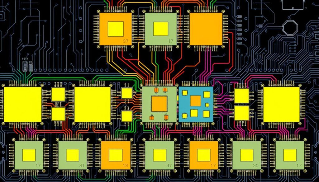
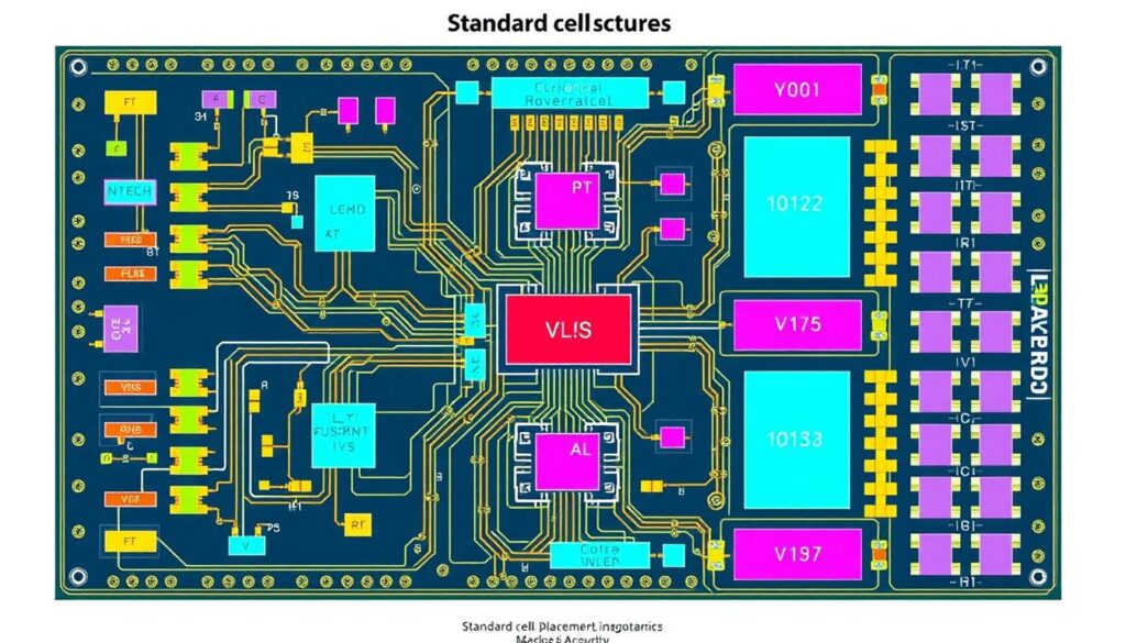
In VLSI design, standard cell placement is key. It finds the best spots for standard cells in an integrated circuit’s core area. The main goals are to cut down on delays, shorten wirelength, make sure it’s routable, and manage power and heat.
This stage is crucial for the circuit’s performance, how well it can be routed, and its power use. It’s vital for making high-quality integrated circuits.
By placing standard cells wisely, the process boosts chip performance and power efficiency. It also improves the design’s quality. This stage is a major part of VLSI design, affecting routing and physical verification. It’s key to the integrated circuit’s success and reliability.
Table of Contents
Understanding Standard Cell Placement Fundamentals
In the world of VLSI design, standard cell placement is key. It affects how well a digital circuit works and how efficient it is. Standard cells are pre-made logic gates with fixed heights and variable widths. They are the building blocks for digital logic functions.
These standardized parts help make design work faster and allow for the reuse of pre-made blocks. This is crucial for improving design efficiency.
What is a Standard Cell?
A standard cell is a pre-made logic gate in a standard cell library. Its design helps use chip area well, making the layout more efficient. Each cell is tested thoroughly for timing and power, ensuring it works as expected.
Core Components of Placement
To place standard cells, you need a few key things. These include the gate-level netlist, design libraries (like the standard cell library), technology files, and design constraints. These are what the placement tool uses to optimize timing, power, and area during physical design.
Role in VLSI Design Flow
After logic synthesis and before routing, standard cell placement happens. It decides where each cell goes on the chip. This step is vital for how fast the chip will run and how well it will work.
The goal is to make the design fast, efficient, and reliable. Placement tries to balance timing, area, power, and congestion to meet these goals.
| Placement Technique | Description |
|---|---|
| Timing-driven Placement | Focuses on optimizing the critical path delays and meeting timing constraints. |
| Congestion-driven Placement | Aims to minimize routing congestion and hotspots, ensuring efficient routing. |
| Power-driven Placement | Targets power optimization, minimizing the overall power consumption. |

Key Placement Objectives and Quality Metrics
In VLSI design, the main goals of standard cell placement are clear. They aim to improve timing optimization, congestion reduction, power efficiency, and area minimization. Finding the right balance between these goals is a big challenge for placement algorithms.
Designers use specific metrics to check the quality of placement. These include total wirelength, critical path delay, and routing congestion. They also look at cell density, pin density, and power consumption. Algorithms try to lower these metrics while following design rules and ensuring the design can be made.
| Placement Objective | Description |
|---|---|
| Timing Optimization | Minimizing the critical path delay to improve circuit performance and meet timing constraints. |
| Congestion Reduction | Preventing routing congestion by optimizing the distribution of cells and interconnects. |
| Power Efficiency | Reducing power consumption through strategic placement of cells and interconnects. |
| Area Minimization | Optimizing the utilization of the chip area to minimize the overall size of the design. |
By focusing on these key objectives and monitoring quality metrics, placement algorithms can create highly optimized VLSI designs. These designs meet the strict needs of today’s electronic systems.
Standard Cell Placement Stages and Methodology
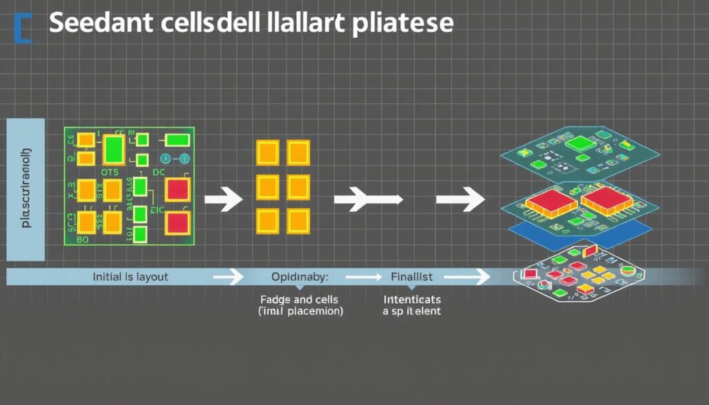
The standard cell placement process has three main stages: global placement, legalization, and detailed placement. These stages work together to place individual cells in the chip’s layout. They aim to use resources efficiently and meet performance goals.
Global Placement Process
The global placement stage creates a rough solution, focusing on timing and congestion. It sets the stage for the rest of the process. Algorithms are used to find the approximate locations of standard cells, aiming to reduce interconnect length and improve timing.
Legalization Requirements
The legalization stage makes sure all standard cells are placed without overlaps. It adjusts cell locations to fit the placement grid, keeping the design’s timing intact. Legalization is key to maintaining the placement solution’s integrity.
Detailed Placement Optimization
The final stage, detailed placement optimization, makes local improvements. It uses incremental optimization techniques like cell swapping and movement. This step addresses timing and congestion issues to meet performance and timing requirements.
Throughout the process, checks and constraints are applied. These ensure the design meets industry standards and foundry requirements. This includes DRC checks, floorplanning, and power optimization strategies.
This comprehensive methodology aims to create an optimized chip layout. It meets performance, power, and area targets, contributing to the success of VLSI design.

Performance and Timing Considerations
Getting standard cells in the right place is key to how well a circuit works and how it meets timing needs. The way cells are placed affects how long it takes for signals to travel between them. This can be a big part of the circuit’s speed.
When placing cells, timing is everything. I need to make sure the circuit meets all its timing needs. This includes how long it takes for signals to set up and hold, and managing clock skew.
Using techniques like useful skew optimization and early clock tree synthesis helps a lot. These methods help keep the clock signal in sync and reduce issues like power loss and electromigration. This makes the circuit run faster and more reliably.
Source Links
- Placement in VLSI Physical Design
- Placement Steps in Physical Design – Team VLSI
- PLACEMENT – VLSI TALKS
- What is a Standard Cell in VLSI? – Maven Silicon
- Non-Overlapping Placement of Macro Cells based on Reinforcement Learning in Chip Design
- Microsoft PowerPoint – lec6.ppt
- Standard cell
- PLACEMENT
- Microsoft PowerPoint – ARM_Artisan_SC_Benchmarking.pptx
- Placement Overview – VLSITutor
- Floorplanning in Physical Design

