Timing constraints are an essential aspect of static timing analysis (STA) in the design of ASICs or FPGAs. In STA, timing constraints are used to validate the timing performance of a design by checking all possible paths for timing violations. This helps optimize circuit performance and ensure reliability.
By properly defining timing constraints, designers can optimize circuit performance and ensure the reliability of their designs. STA breaks down a design into timing paths, calculating the signal propagation delay along each path, and checking for violations of timing constraints. This allows designers to identify potential issues and make necessary adjustments to meet timing requirements. Understanding timing constraints is crucial in the overall design and optimization of electronic circuits.
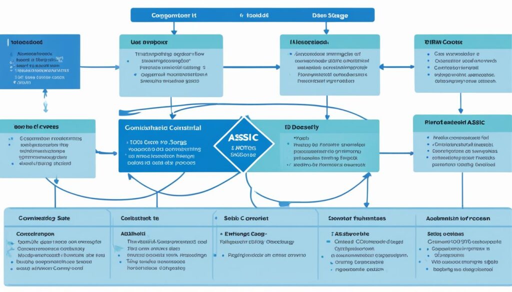
Throughout the ASIC design flow, timing constraints play a critical role. From the logical design phase to the physical design phase, timing constraints are applied during synthesis, design for testability (DFT), equivalence checking, and static timing analysis. Properly defining timing constraints at each stage ensures that the design meets timing requirements and can be successfully manufactured.
Timing constraints are a fundamental aspect of circuit design, allowing designers to optimize performance and ensure reliability. By performing static timing analysis and properly constraining designs, we can validate the timing performance of our circuits, optimize circuit performance, and meet design specifications. Through a comprehensive understanding of timing constraints, we can achieve successful tapeouts and deliver high-quality electronic products.
Table of Contents
How does STA work?
In Static Timing Analysis (STA), the design undergoes a meticulous breakdown into timing paths. These timing paths are the key components that enable us to evaluate and analyze the performance of a circuit. Each timing path consists of three essential elements: the startpoint, the combinational logic network, and the endpoint.
Timing Paths
The startpoint is where data is launched either by a clock edge or needs to be available at a specific time. It sets the initial conditions for the data flow within the circuit. The combinational logic network represents the intermediate logic gates between the startpoint and the endpoint. These logic gates do not retain any memory or internal state, allowing for instantaneous data propagation. Finally, the endpoint is where data is captured either by a clock edge or needs to be available at a specific time. It signifies the final result of the circuit operation.
Different types of paths are taken into account during STA, including clock paths, clock-gating paths, and asynchronous paths. Clock paths are the most commonly analyzed paths in STA, as they are crucial for maintaining the synchronization and reliable operation of the circuit. Clock-gating paths involve the enablement or disabling of clocks for certain sections of the circuit, providing power-saving benefits. Asynchronous paths exist in the presence of signals that do not rely on specific clock edges for their operation, requiring special consideration during the analysis.
Calculating Delays and Checking Constraints
Once the design is broken down into timing paths, an STA tool is utilized to calculate the delay along each path. By determining the delay, we can gain insights into the timing characteristics of the circuit. The tool then compares the calculated delay against a set of timing constraints defined by the designer.
The timing constraints serve as the benchmark for the circuit’s performance. They ensure that the circuit meets the specified timing requirements and operates within the desired parameters. Any violations of the timing constraints in the timing paths may indicate potential malfunctions or performance issues that need to be addressed.
Optimizing Circuit Performance
Static Timing Analysis plays a crucial role in optimizing circuit performance. By analyzing the timing paths and identifying timing violations, designers can make informed decisions to enhance the circuit’s overall performance. This may involve modifying the circuit’s architecture, adjusting the timing constraints, or revising the design implementation.
Moreover, STA also enables designers to explore different optimization techniques such as pipeline insertion, clock tree restructuring, and gate resizing. These optimizations aim to improve the circuit’s speed, power efficiency, and area utilization.
In summary, Static Timing Analysis is an essential tool in the design and evaluation of electronic circuits. By breaking down the design into timing paths, calculating delays, and checking against timing constraints, we can identify potential issues and optimize circuit performance effectively.
Timing Constraints in the ASIC Design Flow.
Timing constraints play a crucial role in the ASIC design flow, ensuring that the design meets timing requirements and can be manufactured successfully. These constraints are applied throughout both the logical and physical design phases, shaping the entire process from start to finish.
Synthesis and Design for Testability (DFT)
In the logical design phase, timing constraints are utilized in various stages, including synthesis and design for testability (DFT). Synthesis is a critical step that converts the Register-Transfer Level (RTL) design into a gate netlist, accounting for timing, power, and area constraints. By defining the appropriate timing constraints during synthesis, designers can optimize the design’s performance and meet the required specifications.
DFT focuses on preparing the design for testability by incorporating scan chains and other test structures. Timing constraints play a crucial role in this stage, ensuring that the design is testable and can be effectively validated using static timing analysis (STA).
Equivalence Checking and Static Timing Analysis (STA)
Equivalence checking verifies the functionality of the gate netlist against the original RTL description. Timing constraints are instrumental in this process, allowing designers to ensure that the functionality of the design is preserved during the synthesis stage.
STA, on the other hand, checks for timing violations without the need for simulations. It analyzes the timing paths within the design and identifies any violations against the defined constraints. By incorporating timing constraints in the STA process, designers can identify and resolve potential timing issues before fabrication.
Physical Design and Signoff STA
In the physical design phase, timing constraints continue to be utilized in various stages. During floor planning, placement, clock tree synthesis, and routing, timing constraints guide the physical implementation process, ensuring that the design’s timing requirements are met. LVS (Layout versus Netlist) verification and DRC (Design Rule Checking) also rely on appropriately defined timing constraints to validate the integrity of the design.
Finally, signoff STA is performed to ensure that all timing constraints have been satisfied and the design is ready for fabrication. By meticulously defining timing constraints at each stage of the ASIC design flow, designers can optimize circuit performance, adhere to timing requirements, and ensure the reliability of their designs.

Types of Timing Constraints.
In the design and optimization of electronic circuits, timing constraints play a crucial role. Designers rely on these constraints to ensure that their circuits meet timing requirements and operate as intended. Different types of timing constraints serve specific purposes and help define the characteristics of various elements within a design.
Clock Constraints
One essential type of timing constraint is clock constraints. Clock constraints are used to specify various characteristics of the clock signal, including its period, duty cycle, skew, latency, and transition time. By defining these parameters accurately, designers can ensure the proper operation and synchronization of their circuits.
Port Delays
Port delays are another important type of timing constraint. They are used to specify the arrival time and required time of signals at input and output ports. By defining the desired arrival time, designers can guarantee that signals are available when needed, while required time constraints ensure that output signals are valid and stable within specific time limits.
Combinational Path Constraints
Combinational path constraints define the maximum and minimum delay of combinational paths within a design. These constraints ensure that signals propagate through the combinational logic network within specified time limits. By properly constraining combinational paths, designers can avoid timing violations and optimize the overall performance of their circuits.
False Path Constraints
False path constraints are used to mark certain paths as irrelevant for timing analysis. These paths are typically associated with non-functional or unused parts of the design. By declaring them as false paths, designers can exclude them from timing analysis and focus resources on critical paths. This helps streamline the timing analysis process and improves efficiency.
Multicycle Path Constraints
Multicycle path constraints allow for paths that take more than one clock cycle from launch to capture. These paths are encountered in designs where specific data transfers or computations require additional time. By defining multicycle path constraints, designers can ensure that these paths meet the necessary timing requirements, accommodating the additional clock cycles required for proper functionality.
By correctly defining and implementing these different types of timing constraints, designers can ensure the correct operation and performance of their electronic circuits. Whether it’s optimizing clock characteristics, specifying port delays, or constraining combinational, false, or multicycle paths, each type of timing constraint plays a vital role in meeting timing requirements and designing reliable circuits.

Conclusion
Timing constraints are a critical component of electronic circuit design and optimization. By properly defining timing constraints and utilizing static timing analysis (STA), we can ensure the timing performance of our designs, optimize circuit performance, and enhance overall reliability.
Throughout the ASIC design flow, timing constraints play an essential role, starting from the logical design phase and extending to the physical design phase. Properly constraining our designs for synthesis and timing analysis is crucial for achieving successful tapeouts and meeting design specifications.
In conclusion, timing constraints are fundamental to circuit design, enabling us to optimize performance and guarantee reliability. By adhering to timing constraints and employing STA techniques, we can validate the timing performance of our circuits, optimize their efficiency, and ensure the reliability of our electronic products.

