


The short answer: a synchronous FIFO is a first-in, first-out buffer where reads and writes use the same clock. It is a small memory plus a write pointer and a read pointer. Making each pointer one bit wider than the address lets you detect empty (pointers equal) and full (addresses equal, wrap bits different) with simple logic. Get the full and empty conditions, the read latency and the simultaneous read-and-write case right, and you have one of the most reused blocks in digital design.
Synchronous FIFOs are everywhere: between pipeline stages, in front of slow interfaces, in bus bridges. They are also the most common “write this on the whiteboard” interview question. Here is how I would design one.
- How it works
- Full and empty, two ways
- Verilog
- Corner cases to test
- Almost-full and almost-empty
Table of Contents
Part 1: How it works
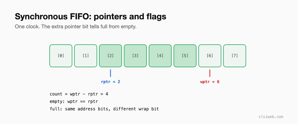
Writes go to the address in the write pointer, which then increments. Reads come from the address in the read pointer, which then increments. Both wrap around at the end of the memory, so the buffer behaves like a circle.
Part 2: Full and empty, two ways
- Extra pointer bit (my preference): use N+1-bit pointers for a 2^N-deep FIFO. Empty when the pointers are equal; full when the low N bits are equal and the top bits differ.
- Counter: keep an occupancy count that increments on write, decrements on read, and stays the same when both happen. Empty when count is 0, full when count equals the depth. Easy to read, but one more adder.
Part 3: Verilog
module sync_fifo #(
  parameter DW = 8,
  parameter AW = 4                 // depth = 2**AW
)(
  input  wire          clk, rst_n,
  input  wire          wr_en,
  input  wire [DW-1:0] wdata,
  output wire          full,
  input  wire          rd_en,
  output reg  [DW-1:0] rdata,
  output wire          empty
);
  reg [DW-1:0] mem [0:(1<<AW)-1];
  reg [AW:0]   wptr, rptr;         // one extra bit for wrap

  wire do_wr = wr_en && !full;
  wire do_rd = rd_en && !empty;

  assign empty = (wptr == rptr);
  assign full  = (wptr[AW] != rptr[AW]) &&
                 (wptr[AW-1:0] == rptr[AW-1:0]);

  always @(posedge clk)
    if (do_wr) mem[wptr[AW-1:0]] <= wdata;

  always @(posedge clk or negedge rst_n)
    if (!rst_n) begin
      wptr  <= 0;
      rptr  <= 0;
      rdata <= 0;
    end else begin
      if (do_wr) wptr <= wptr + 1'b1;
      if (do_rd) begin
        rdata <= mem[rptr[AW-1:0]];  // data valid the cycle after rd_en
        rptr  <= rptr + 1'b1;
      end
    end
endmodule
This version has a registered read: data appears on the cycle after rd_en. A first-word fall-through (FWFT) FIFO instead shows the next word on rdata as soon as it is available. Both are common; just be clear which one you are building.
Part 4: Corner cases to test
- Write when full and read when empty: both must be ignored, not corrupt the pointers.
- Read and write in the same cycle, including when empty and when full.
- Wrap-around: fill, drain and refill so both pointers wrap several times.
- Reset in the middle of traffic.
Simultaneous read and write when empty is a classic trap: with the logic above, the write happens and the read is ignored, which is correct for a registered-read FIFO.
Part 5: Almost-full and almost-empty
Many designs add almost-full and almost-empty flags (for example, count at or above a threshold) so the producer or consumer can react a few cycles early, which helps when there is pipeline latency in the control path.
Practise this on VLSI Forge
I built VLSI Forge so you can write RTL in your browser, run it on a real simulator and check every signal in the waveform. Free, nothing to install.
Once you are comfortable with this, move on to the asynchronous FIFO, where the two pointers live in different clock domains.
FAQ
Why is the FIFO depth usually a power of two?
Pointers then wrap naturally when they overflow, and the full/empty logic stays simple. Other depths need explicit wrap logic.
What is a first-word fall-through FIFO?
A FIFO where the oldest word is already on the output when the FIFO is not empty, so the read signal acknowledges it rather than requesting it.
How deep should my FIFO be?
That depends on burst sizes and rates. See FIFO depth calculation for worked examples.
Can I use a synchronous FIFO between two clocks?
No. If the clocks are different and unrelated, you need an asynchronous FIFO with Gray-coded pointers.
