

The short answer: reset domain crossing (RDC) problems happen when a flop is reset asynchronously while a flop it feeds, in another reset domain, is not being reset. The reset can change the first flop’s output at any moment, so the second flop can capture it at a bad time and go metastable, even if both are on the same clock. The usual fixes are a reset synchroniser per domain (assert asynchronously, release synchronously), careful reset ordering, and isolating or gating crossing signals while one side is in reset.
Most engineers learn CDC first and only meet RDC later, often through a tool report they do not understand. RDC is really the reset version of the same problem: a signal changing asynchronously relative to the flop that samples it. Here is how I would explain it.
- Reset synchronisers: asynchronous assert, synchronous release
- What a reset domain crossing is
- How to fix RDC issues
- Synchronous vs asynchronous reset
- How RDC is checked
Table of Contents
Part 1: Reset synchronisers: asynchronous assert, synchronous release
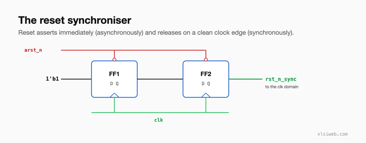
Asserting reset asynchronously means the design resets immediately, even with no clock running. Releasing it through two flops means every flop in the domain leaves reset on the same clean clock edge, avoiding recovery and removal timing problems.
module reset_sync (
  input  wire clk,
  input  wire arst_n,       // asynchronous reset in
  output wire rst_n_sync    // asserted async, released sync
);
  reg r1, r2;
  always @(posedge clk or negedge arst_n)
    if (!arst_n) {r2, r1} <= 2'b00;
    else         {r2, r1} <= {r1, 1'b1};
  assign rst_n_sync = r2;
endmodule
Part 2: What a reset domain crossing is
Large chips have several reset domains: power-on reset, a warm reset for the CPU, software resets for individual blocks, and resets for power domains that switch on and off. A reset domain crossing exists when a flop in one reset domain drives a flop in another.
Suppose block A is reset by software while block B keeps running. When A’s flops are asynchronously reset, their outputs change at a moment that has nothing to do with B’s clock edge. If B samples that output, it can go metastable, exactly like a CDC problem, even on the same clock.
Part 3: How to fix RDC issues
- Order your resets: reset the receiving domain at the same time as, or before, the sending domain, so the receiver is not sampling when the sender resets.
- Isolate the crossing: gate or hold the crossing signals at a safe value while the sending domain is in reset.
- Synchronise the data: treat the crossing like a CDC and pass it through a synchroniser.
- Use synchronous reset assertion for the sending flops where the design allows it.
Part 4: Synchronous vs asynchronous reset
| Synchronous reset | Asynchronous reset | |
|---|---|---|
| Takes effect | On the next clock edge | Immediately |
| Needs a running clock | Yes | No |
| Timing | Normal setup and hold on the reset path | Recovery and removal checks on de-assertion |
| Common use | Datapaths, FPGA designs | Control logic, chips that must reset without a clock |
Many ASIC teams use asynchronous assertion with synchronous de-assertion (the reset synchroniser above) for control logic, and avoid resetting large datapaths that do not need it, which saves area and power.
Part 5: How RDC is checked
Like CDC, RDC bugs are rarely found by simulation. Dedicated RDC analysis (usually part of the same CDC tools) identifies reset domains, finds crossings between them and checks for ordering, isolation or synchronisation. See CDC and RDC verification.
Practise this on VLSI Forge
I built VLSI Forge so you can write RTL in your browser, run it on a real simulator and check every signal in the waveform. Free, nothing to install.
FAQ
Can RDC issues happen on a single clock?
Yes. The problem is the asynchronous reset changing a flop’s output at an arbitrary time, so it can happen even when both flops share a clock.
Why do we need one reset synchroniser per clock domain?
Each domain must release reset on its own clean clock edge. A reset synchronised to one clock is asynchronous to every other clock.
What are recovery and removal checks?
The asynchronous-reset equivalents of setup and hold: reset must be released far enough from the clock edge so the flop leaves reset cleanly.
Should every flop have a reset?
No. Control flops usually need one; many datapath flops do not, as long as their values are not used before valid data arrives.
