

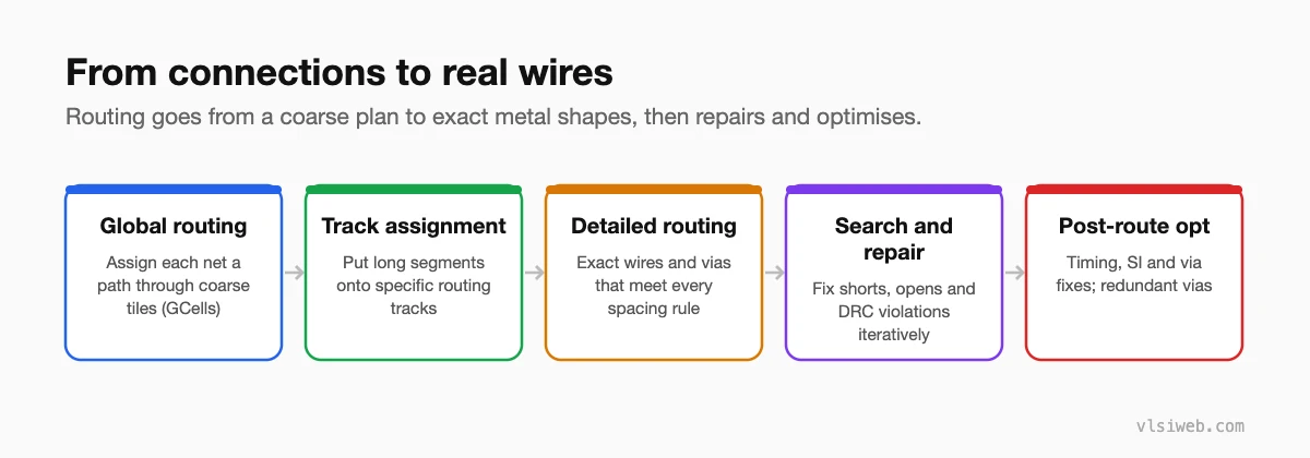
The short answer: Routing creates the actual metal wires and vias for every net after placement and CTS. Global routing divides the block into coarse tiles and plans each net’s path, revealing congestion; track assignment and detailed routing then produce exact shapes that obey every spacing, width and via rule; search-and-repair fixes the remaining violations. Clock nets are usually routed first with special rules. Post-route optimisation fixes timing and signal integrity, and redundant (double) vias are added for reliability and yield.
Routing is where the design becomes real geometry. Modern routers are very good, but they can only route what placement and the floorplan make routable. This post combines my older posts on global vs detailed routing, routing algorithms and via optimisation.
- The steps
- Global vs detailed routing
- How routers work (briefly)
- Layers and preferred directions
- Vias
- Special nets
- After routing
Table of Contents
Part 1: The steps
Part 2: Global vs detailed routing
| Global routing | Detailed routing | |
|---|---|---|
| Works on | Grid of GCells (tiles) | Individual routing tracks and vias |
| Output | Rough path per net, congestion map | Exact wires that meet design rules |
| Speed | Fast | Slow; most of the routing runtime |
| Main metric | Overflow (demand vs capacity) | DRC violations, opens, shorts |
Part 3: How routers work (briefly)
- Maze routing (Lee’s algorithm) expands a wave from the source until it reaches the target; it always finds a path if one exists, but is slow on big grids, so it’s used locally.
- Line-probe routing extends lines instead of cells; faster, but may miss paths.
- Steiner trees connect multi-pin nets with minimum total length, adding branch points.
- Rip-up and reroute removes and re-routes nets that cause congestion or violations, again and again, until the design converges.
Part 4: Layers and preferred directions
Each metal layer has a preferred direction (alternating horizontal and vertical). Lower layers are thin with tight pitch, for local connections; upper layers are thick and low-resistance, for long nets, clocks and power. Advanced nodes add strict rules: fixed track patterns, multiple patterning colours, and line-end and via spacing rules that make routing much harder.
Part 5: Vias
- Each via adds resistance and is a reliability risk; long nets with many layer changes get slower.
- Redundant (double) vias replace single vias where there’s room, improving yield and electromigration margin.
- Via pillars or stacked vias on critical nets reduce resistance at advanced nodes.
- Via rules (enclosure, spacing, cut patterns) are a large part of advanced-node DRC.
Part 6: Special nets
Clock nets are routed first, often with non-default rules: double width and spacing, or shielding with ground wires, to reduce crosstalk and variation. Critical and high-speed nets can get similar rules. Power nets are already in place from power planning.
Part 7: After routing
The design is extracted with real parasitics, and timing, crosstalk, IR drop and DRC are checked. Remaining issues are fixed with post-route optimisation and ECOs. More in parasitics and crosstalk and timing closure and ECOs.
Practise this on VLSI Forge
I built VLSI Forge so you can write RTL in your browser, run it on a real simulator and check every signal in the waveform. Free, nothing to install.
Physical Design problems · Static Timing Analysis problems
Previous in my physical design series: Clock tree synthesis. Next: Parasitics and crosstalk.
FAQ
What is the difference between global and detailed routing?
Global routing plans each net’s path through coarse tiles and estimates congestion; detailed routing creates the exact wires and vias that meet the design rules.
Why are clock nets routed first?
So they get the best routing resources and special rules like extra spacing or shielding before signal nets fill the tracks.
What is a redundant via?
An extra via placed alongside a single via on the same connection, improving reliability and yield.
What is rip-up and reroute?
An iterative technique where nets causing conflicts are removed and re-routed until violations are resolved.
