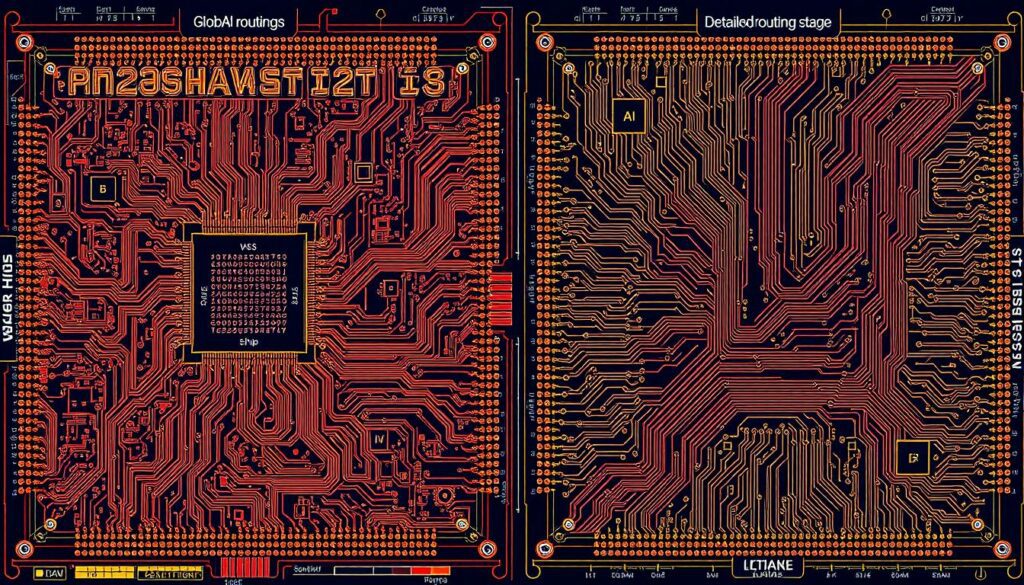
In VLSI design and chip layout, routing is key. It shapes the circuit’s final form. The process splits into two main parts: global routing and detailed routing. Knowing these differences is vital for chip design.
Global routing starts the process. It divides the chip into logical parts called buckets. This stage estimates the needed paths for each connection. It aims to fit all connections within the available resources.
Detailed routing comes next. It’s about making the actual wires for the chip. This step must follow strict rules for wire width and spacing. It ensures the circuit works right.
The two-stage method helps with complex designs. It tackles the big picture first, then the details. This way, designers manage the vast number of connections and rules.
Table of Contents
Understanding Basic Routing Concepts in VLSI Design
Routing is key in VLSI design, making sure wires connect the right pins. It follows rules for making chips. The process turns circuit plans into real wires and paths.
Core Components of Chip Routing
The main parts for routing include a placed layout and a netlist. There’s also a timing budget and design rules. The goal is to create wire connections that meet these rules and goals.
The Two-Stage Routing Approach
The routing process has two main steps: global and detailed routing. Global routing picks the best paths for each net. Detailed routing then fixes any issues and makes the layout better.
Design Rules and Constraints
Many rules guide the routing process. These include how dense the wiring can be and where wires can go. These rules help make sure the chip works right.

Global Routing vs Detailed Routing: Key Differences
In the world of VLSI design, two key stages are global routing and detailed routing. They both aim to connect circuit components but use different methods. These methods are crucial for the design’s success.
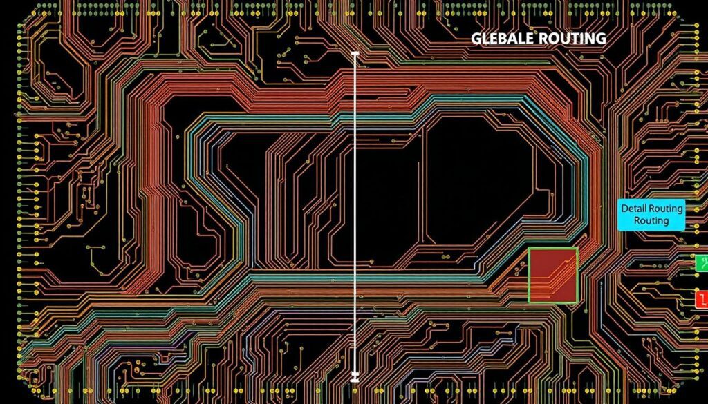
Global routing starts by dividing the design into tiles called global routing cells (gcells). It looks for the best paths between these tiles to meet design goals like wirelength and timing. This stage uses a global routing graph to plan these paths.
Detailed routing comes next. It focuses on laying out the exact paths for each net within the tiles. It ensures the wires and vias fit without causing problems. This stage is all about the fine details of the layout.
The main difference is in their focus. Global routing looks at the big picture, aiming for overall design goals. Detailed routing gets into the small details, making sure everything works right.
| Global Routing | Detailed Routing |
|---|---|
| Determines tile-to-tile paths for all nets | Assigns actual tracks and vias for nets within the tile-to-tile path |
| Optimizes objectives like total wirelength and circuit timing | Ensures the feasibility and correctness of the final circuit layout |
| Uses a global routing graph with gcells as nodes and tile boundaries as edges | Guided by the global routing paths, determines the exact geometric layout of metal wires and vias |
Understanding the roles of global and detailed routing helps VLSI designers. They can improve both the overall plan and the detailed layout of the chip.
Global Routing: Process and Methodology
The global routing stage in VLSI design is key. It defines routing regions and assigns nets to them. This two-stage process helps manage the complexity of modern chip design.
Tile-Based Partitioning
Global routing divides the chip into “buckets” or “tiles”. This method makes resource estimation and management easier. It also helps analyze congestion in each region.
Resource Estimation and Management
The global router estimates available routing resources. It looks at the number of tracks on each metal layer and the resources needed for each net. This helps spot areas where resources are short.
Congestion Analysis
If the router finds high congestion, it focuses on those areas. It aims to route as many nets as possible. This ensures each area meets its capacity and design rules.
| Metric | Value |
|---|---|
| Routing Tracks Capacity | 1200 tracks per tile |
| Nets Routed Successfully | 95% |
| Congestion Reduction | 20% |

Tile-based partitioning, resource estimation, and congestion analysis are crucial. They set the stage for successful detailed routing. This ensures efficient use of resources, reduces overflow, and tackles congestion challenges.
Detailed Routing: Implementation and Techniques
Detailed routing is key in VLSI design. It creates the actual wire connections between each net’s pins. This involves placing wires on metal layers and using vias to move between them. It must follow the design rules set by chip foundries.
If the routing tool can’t meet these rules or if there’s too much wire density in one area, it’s called congested. This makes it hard to complete the design.
The aim of detailed routing is to make a high-quality solution. It tries to balance wire length, via count, and other needs. This is tough because technology keeps getting more complex.
Good detailed routing algorithms are vital in VLSI design. They affect how well the circuit works and if it can be made. These algorithms use global routing info and tech node factors to make strong, efficient connections.
The divide-and-conquer method helps deal with today’s complex routing. It makes the routing process more efficient.

