In the world of VLSI chip design, physical design is key. It turns a circuit description into a real, physical layout. This involves changing a netlist, a logical map of parts, into a GDSII form. This form affects the chip’s performance, size, reliability, power use, and how well it’s made.
During physical design, all parts, like macros and transistors, get placed and connected. This careful work makes sure the circuit works well in real life. It turns the logical plan into a working chip.
Physical design is very important in VLSI. It affects how well the chip works and its features. Designers work to make the chip faster, use less power, and have fewer mistakes. This makes the chip better and more reliable.
As VLSI chips get more complex, with over 50 billion transistors in one chip, design is more critical. Designers use tools like Synopsys ICCI and Cadence Encounter to make chips that meet industry needs. They aim to create efficient and high-performance chips.
Table of Contents
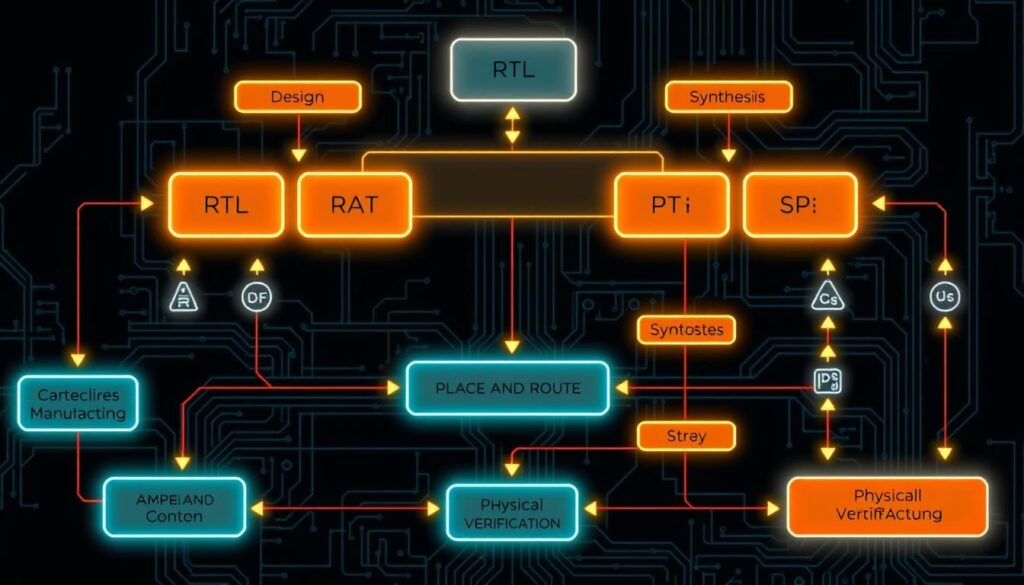
Understanding VLSI Physical Design Flow
The VLSI physical design flow starts with a gate-level netlist. This netlist comes from the ASIC flow and netlist synthesis. It turns RTL designs into gate-level specs for silicon implementation. Design constraints guide the process, ensuring the design meets performance, area, and power targets.
Technology libraries and files are key in the VLSI physical design flow. They include logical and physical libraries, technology files, and TLU+ files. These resources give vital information for the design process. EDA tools from Synopsys, Cadence, and Mentor Graphics are used for tasks like place and route, timing analysis, and physical verification.
Gate-Level Netlist and Synthesis
The flow starts with a gate-level netlist from synthesis. This netlist turns RTL designs into gate-level representations. The synthesis process considers design constraints, ensuring the netlist meets performance, area, and power targets.
Design Constraints and Requirements
Design constraints and requirements are crucial in the physical design process. They include clock frequency, timing margin, and maximum capacitance. These parameters ensure the design meets performance and reliability targets. Static Timing Analysis (STA) tools help identify timing issues, allowing for layout optimization.
Technology Libraries and Files
Technology libraries and files are essential for the VLSI physical design flow. They include logical and physical libraries, technology files, and TLU+ files. These resources provide information on input capacitances, timing arcs, and other critical parameters. Regular libraries store this information, helping the design team accurately model and optimize the design.
| Design Requirement | Description |
|---|---|
| Clock Frequency | The target clock frequency for the design, which affects the timing constraints and optimization goals. |
| Timing Margin | The desired timing margin to ensure the design meets the performance targets and can operate reliably. |
| Maximum Capacitance | The maximum allowable capacitance on a net, which impacts signal integrity and power consumption. |

Key Components of Physical Design
The physical design stage in VLSI is key. It turns the logical circuit design into a detailed layout for making chips. This stage includes several important parts that work together. They aim to improve chip performance, area, and power use.
Floorplanning and Partitioning
Floorplanning decides how sub-circuits, modules, and blocks fit in the chip area. It tries to use the chip well, reduce routing problems, and boost performance. Partitioning breaks the circuit into smaller parts. This makes the design easier to handle.
Placement and Optimization
Placement finds where each cell goes in the chip. It aims to meet timing needs, cut down on delays, and lower power use. There are different steps to improve the design, like pre-placement, in-placement, and post-placement.
Clock Tree Synthesis (CTS)
Clock Tree Synthesis deals with clock signals across the chip. It works to cut down clock skew, lower power use, and keep signals strong. CTS uses buffering, gating, and routing to meet timing needs.
Routing and Connectivity
Routing sets up electrical connections between chip components. It involves global routing for main paths and detailed routing for exact routes. This is done using metal layers and tracks.
Power Planning
Power planning is about spreading out power and ground nets in the chip. It helps with efficient power delivery, manages power use, and avoids issues like voltage drops and electromigration.
These key parts of physical design work together to create a chip layout that meets performance, area, and power goals. Optimizing and integrating these elements is vital for successful VLSI circuit implementation.
Physical Design Stages and Implementation
The process of making a VLSI (Very Large Scale Integration) chip involves many important steps. These steps work together to make the chip better in performance, power use, and size. These are key to making an integrated circuit successful.
Floorplanning and Chip Planning
The first step is floorplanning. Here, the size and shape of the chip, where cells and I/O pins go, are planned. This planning aims to use less space, improve performance, and make power distribution easier.
Placement and Optimization
Placement is a key step. It places standard cells in the best spots for timing, congestion, and power. The goal is to cut down wire length, reduce congestion, and boost circuit timing analysis and signal integrity.
Clock Tree Synthesis (CTS)
Clock Tree Synthesis (CTS) makes sure all parts of the chip get the clock signal at the same time. This helps keep the design running smoothly and reliably by ensuring everything is in sync.
Routing and Connectivity
The last step is routing. It connects different parts of the chip using metal layers and vias. Routing aims to meet timing needs, avoid errors, and cut down wire length. This helps optimize chip area and congestion management.
Throughout these steps, the design is always being improved for area, timing, power, and performance. This ensures the final chip meets all the needed specs and requirements.

Impact of Physical Design on Circuit Performance
The physical design of VLSI is key to a circuit’s performance, power use, reliability, and how well it’s made. Choices made during design can greatly affect the circuit’s final traits.
Performance and Area Optimization
Where components are placed and connected on the chip affects how well it works. Longer paths can slow down signals, hurting the circuit’s speed. To fix this, designers use techniques to shorten paths and speed up signals.
They also try to use the chip space wisely. This means finding a balance between how big the circuit is and how fast it can go. This balance helps make the most of the chip’s area.
Power Management
Power use is a big deal in VLSI design, more so for devices that need to be portable. Designers use methods like changing voltage levels and turning off parts of the circuit to save power. But, making transistors smaller can make them leak more power.
So, designers have to be careful with these issues. They need to find ways to make circuits use less power without losing performance.
Reliability and Yield Factors
Design choices also affect how reliable and well-made the circuit is. Where components are placed and how they’re connected can make the circuit more prone to problems. Designers use methods to make the circuit more reliable and easier to test.
They also focus on making sure the circuit works as expected. This ensures the final product meets all the needed standards and performs well.
Source Links
- what is physical design
- Steps In VLSI Physical Design Flow
- VLSI Physical Design Flow
- Physical Design Flow – Maven Silicon
- Physical design (electronics)
- What are the Steps in Physical Design? – Maven Silicon
- Conceptual, Logical and Physical design
- VLSI: Physical Design (PD P1) — Introduction to PD
- Basics of physical design
- How Can Physical Design Optimize VLSI Performance?
- Understanding the Importance of Prerequisites in the VLSI Physical Design Stage
- 5 Common Challenges in VLSI Design and How to Overcome Them – Maven Silicon

