

The short answer: PCIe interviews usually walk down the protocol stack: topology (root complex, switches, endpoints), the three layers, TLP types and posted vs non-posted requests, the ACK/NAK replay mechanism, credit-based flow control, encoding and generations, link training through the LTSSM, configuration space and BARs, interrupts (MSI and MSI-X), ordering rules, power states and error reporting. Design roles focus on the controller logic; verification roles add VIP, compliance and error injection.
PCIe is a deep protocol, and nobody expects you to know the whole specification. What interviewers want is a clear mental model of how a request travels from one device to another, and the reasons behind the main mechanisms.
I’ve ordered the questions in the same way: from the big picture down to the details. If you’re also preparing for on-chip buses, see my AXI interview questions.
- Architecture and layers
- Transactions
- Reliability and flow control
- Link training and power
- Configuration and interrupts
Table of Contents
Part 1: Architecture and layers
1. What is PCIe?
PCI Express is a serial, point-to-point, full-duplex interconnect. A link is made of 1 to 16 lanes (x1 to x16), and each lane is a pair of differential signals in each direction. It replaced the shared parallel PCI bus, keeping PCI’s software model (configuration space, memory-mapped devices).
2. What are the components in a PCIe topology?
The root complex connects the CPU and memory to the PCIe hierarchy. Switches fan one link out to several. Endpoints are the devices (SSDs, GPUs, NICs). Bridges connect PCIe to other buses.
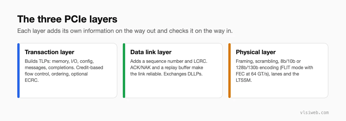
3. What does each layer do?
The transaction layer creates and decodes TLPs and handles flow control and ordering. The data link layer makes the link reliable with sequence numbers, LCRC and ACK/NAK. The physical layer handles encoding, scrambling, lane management and link training.
4. How have PCIe generations changed?
| Generation | Rate per lane | Encoding | About x1 per direction |
|---|---|---|---|
| Gen1 | 2.5 GT/s | 8b/10b | 250 MB/s |
| Gen2 | 5 GT/s | 8b/10b | 500 MB/s |
| Gen3 | 8 GT/s | 128b/130b | 1 GB/s |
| Gen4 | 16 GT/s | 128b/130b | 2 GB/s |
| Gen5 | 32 GT/s | 128b/130b | 4 GB/s |
| Gen6 | 64 GT/s | PAM4, FLIT mode with FEC | 8 GB/s (before FLIT overhead) |
Gen3 moved to 128b/130b because 8b/10b wastes 20% of the bandwidth. Gen6 switched to PAM4 signalling, which needs forward error correction, so data moves in fixed-size FLITs.
Part 2: Transactions
5. What types of TLPs are there?
Memory read and write, I/O read and write (legacy), configuration read and write, messages (interrupts, power management, errors), and completions, which return data or status for non-posted requests.
6. What is the difference between posted and non-posted requests?
Posted requests (memory writes and messages) don’t get a completion; the sender moves on. Non-posted requests (memory reads, I/O and configuration requests) need a completion. Posted writes are why PCIe write bandwidth is so efficient.
7. What is in a TLP?
A 3-DW or 4-DW header (4 DW for 64-bit addresses) with type, length, requester ID, tag and attributes; an optional data payload; and an optional end-to-end CRC (ECRC). The data link layer adds a sequence number and LCRC, and the physical layer adds framing.
8. How are completions matched to requests?
Each non-posted request carries the requester ID (bus, device, function) and a tag. The completer copies them into the completion, so the requester can match it, even when completions arrive out of order or are split into several parts.
9. What are max payload size and max read request size?
Max payload size limits the data in any one TLP; max read request size limits how much a single read can ask for. Large reads are returned as several completions. Both are set during enumeration to values every device on the path supports.
10. What are the PCIe ordering rules in short?
Posted writes must not be passed by later reads or by other posted writes (unless relaxed ordering allows it), which is what makes the producer-consumer model work: a read that follows a write sees the written data. Relaxed ordering and ID-based ordering attributes let devices loosen this where it’s safe, for performance.
Part 3: Reliability and flow control
11. How does the ACK/NAK protocol work?
The transmitter gives each TLP a sequence number and keeps a copy in a replay buffer. The receiver checks the LCRC and sequence number and returns ACK or NAK DLLPs. On a NAK, or if the replay timer expires, the transmitter resends from the replay buffer. ACKed TLPs are removed.
12. How does credit-based flow control work?
The receiver advertises credits for each buffer type (posted, non-posted and completion, each with header and data credits). The transmitter only sends a TLP if it has enough credits, so receive buffers never overflow and no TLP is dropped for lack of space. The receiver returns credits with UpdateFC DLLPs as it frees space.
13. What is AER?
Advanced Error Reporting classifies errors as correctable (fixed by hardware, such as a replayed TLP), uncorrectable non-fatal (a transaction failed but the link is fine) or fatal (the link is unreliable), and logs details in extended configuration registers.
14. What completion status codes exist?
Successful Completion (SC), Unsupported Request (UR), Completer Abort (CA), and Configuration Request Retry Status (CRS), which a device uses when it isn’t ready yet after reset.
Part 4: Link training and power
15. What is the LTSSM?
The Link Training and Status State Machine brings the link up. The main states are Detect (is a receiver present?), Polling (bit and symbol lock), Configuration (lane width, lane numbering), L0 (normal operation) and Recovery (retraining, speed changes and equalisation). There are also power states (L0s, L1, L2) and special states like Hot Reset, Disabled and Loopback.
16. Why is equalisation needed from Gen3?
At 8 GT/s and above, channel loss distorts the signal badly. During Recovery the two ends exchange presets and adjust transmitter and receiver equalisation until the eye is open enough for a low bit error rate.
17. What are the link power states?
L0 is active. L0s is a quick, low-saving standby for one direction. L1 saves more power with a longer exit latency, and L1.1 and L1.2 substates save more again. L2 and L3 are for when main power is removed. ASPM (Active State Power Management) lets hardware enter L0s and L1 on its own when the link is idle.
Part 5: Configuration and interrupts
18. What is in configuration space?
Each function has 4 KB: the first 256 bytes are PCI-compatible (vendor and device ID, command and status, BARs, capability pointers) and the rest is extended space for capabilities like AER. Endpoints use a Type 0 header; bridges and switch ports use Type 1.
19. How does software find the size of a BAR?
It writes all 1s to the BAR and reads it back. The device hardwires the low address bits to 0, so the number of zero bits gives the size. For example, a read-back of 0xFFFF_F000 (ignoring the type bits) means a 4 KB region.
20. How does enumeration work?
The root complex scans the hierarchy depth first with configuration reads, finds each device by reading its vendor ID, assigns bus numbers to bridges, then sizes and assigns BARs and enables the devices.
21. What is the difference between INTx, MSI and MSI-X?
INTx emulates the old PCI interrupt wires with messages and is shared. MSI sends an interrupt as a memory write to an address the OS provides, with up to 32 vectors. MSI-X supports up to 2048 vectors, each with its own address, data and mask, held in a table in a BAR. Modern devices use MSI-X.
22. How would you verify a PCIe controller?
- Use a PCIe VIP as the link partner, with protocol checkers enabled.
- Cover the LTSSM thoroughly: every state, speed change, width change and recovery path.
- Inject errors: bad LCRC, NAKs, replay timeouts, malformed TLPs, completion timeouts.
- Stress flow control with small credit counts and many outstanding requests.
- Run the relevant compliance checks before tape-out.
Practise this on VLSI Forge
I built VLSI Forge so you can write RTL in your browser, run it on a real simulator and check every signal in the waveform. Free, nothing to install.
FAQ
How much of the PCIe specification should I know?
The layers, TLP types, ACK/NAK, flow control, the main LTSSM states, configuration space and MSI-X cover most interviews. Deeper physical layer questions are for PHY roles.
Is CXL asked in PCIe interviews?
Increasingly. CXL runs over the PCIe physical layer from Gen5 and adds protocols for cache coherency and memory expansion. Knowing that relationship is usually enough.
What is the most common PCIe interview question?
Posted vs non-posted requests, followed by how flow control credits work.
Do design and verification interviews differ for PCIe?
Yes. Design interviews focus on controller micro-architecture (buffers, replay, credits). Verification interviews focus on VIP, checkers, coverage and error injection.
