

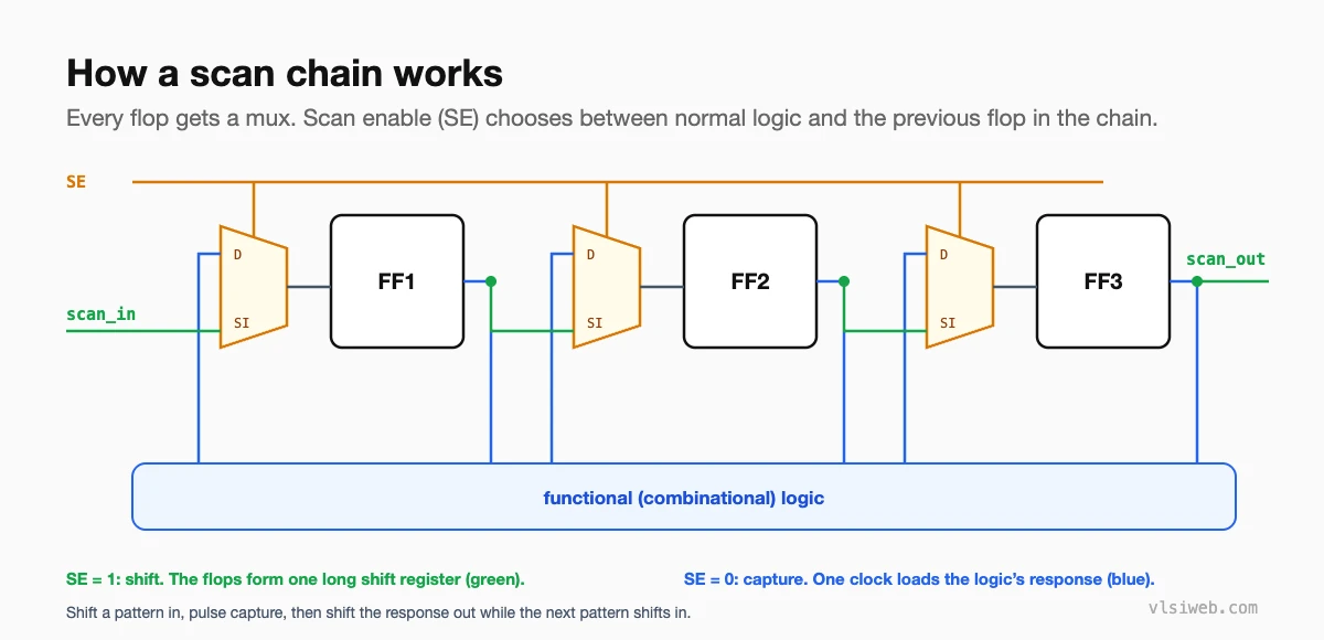
The short answer: DFT interviews cover why we test chips (manufacturing defects, not design bugs), fault models (stuck-at, transition, path delay, cell-aware), scan design and test DRC rules, ATPG and coverage, at-speed testing with on-chip clock controllers, scan compression, memory BIST and repair, logic BIST, and JTAG boundary scan. The scan shift-and-capture picture is the base for almost every question.
DFT is a smaller field than design or verification, but it’s a great career: every chip needs it, and good DFT engineers are always in demand. Interviews mix concept questions with very practical ones, like “why is my coverage low?”
If you want to know what the job looks like day to day, read my post on the DFT engineer role.
- Basics and fault models
- Scan design
- ATPG and coverage
- BIST and JTAG
Table of Contents
Part 1: Basics and fault models
1. What is DFT, and why do we need it?
Design for testability adds logic that lets us test every manufactured chip for defects quickly and cheaply. Verification finds design bugs before tape-out; DFT finds manufacturing defects (shorts, opens, weak transistors) in each chip after fabrication. Without it, testing a modern chip from its pins alone would be practically impossible.
2. What are controllability and observability?
Controllability is how easily you can set a node to 0 or 1 from the chip’s inputs. Observability is how easily you can see a node’s value at the outputs. Scan makes almost every flop both controllable and observable, which turns a hard sequential test problem into a much easier combinational one.
3. What is the stuck-at fault model?
It assumes a node is permanently stuck at 0 or 1. To detect stuck-at-0 on a node, you drive it to 1 and propagate the result to an observable point. It’s simple, but it catches a large share of real defects, which is why it’s still the base of every test.
4. What are transition and path delay faults?
A transition fault models a node that is too slow to rise or fall, and needs two patterns: one to set the initial value and one to launch the transition, captured at functional speed. Path delay faults model an accumulated delay along a specific path, usually used for a few critical paths.
5. What is cell-aware testing?
It models defects inside standard cells, based on transistor-level analysis of each cell’s layout, instead of only at cell pins. It catches defects that stuck-at and transition patterns miss, and is common for automotive and other low-DPPM products.
Part 2: Scan design
6. How does scan testing work?
Each flop is replaced with a scan flop: a mux in front of the D input selects between the functional data and the scan input. In shift mode (SE = 1) the flops form chains, so you can load any pattern. In capture mode (SE = 0) one clock pulse captures the logic’s response. Then you shift the response out while shifting the next pattern in.
7. Why is shift usually slower than functional speed?
Scan chains are not timed for full speed, and all flops toggling at once in shift mode draws a lot of power, which causes IR drop and false failures. So shift often runs at tens of MHz, while capture can be at-speed for transition tests.
8. What are the main scan DRC rules?
- Clocks of scan flops must be controllable from top-level pins in test mode.
- Asynchronous sets and resets must be held inactive during shift.
- No combinational loops, or they must be broken in test mode.
- Latches must be transparent or made scannable.
- Tri-state buses must have no contention during test.
9. What is a lockup latch?
A latch placed between two parts of a scan chain that are on different clocks or have large clock skew. It holds the data for half a cycle so the shift path doesn’t have a hold violation.
10. Why are scan chains reordered after placement?
Chain order from synthesis ignores where the flops end up, so connecting them in that order would add a lot of long wires. Reordering by physical location reduces wiring and congestion. The ATPG tool must be given the final order.
11. How do clock-gating cells affect scan?
An integrated clock gate stops the clock when its enable is low, which would stop scan shifting too. ICG cells therefore have a test enable pin, driven by scan enable or test mode, that forces the clock on during shift.
Part 3: ATPG and coverage
12. What is ATPG?
Automatic test pattern generation: a tool finds input patterns that detect each fault and predicts the expected response. Common tools are Synopsys TestMAX ATPG (TetraMAX) and Siemens Tessent.
13. What is the difference between fault coverage and test coverage?
Fault coverage is detected faults over all faults. Test coverage excludes faults that can’t be tested by design (untestable or redundant), so it’s usually higher and is what most teams report.
14. Why might coverage be low?
Uncontrollable clocks or resets, black boxes such as memories and analog blocks, X-sources that corrupt responses, non-scan flops, and logic that is only controlled by constants in test mode. The ATPG tool’s DRC report usually points straight at the cause.
15. What are launch-on-capture and launch-on-shift?
Both are ways to apply at-speed transition tests. In launch-on-shift, the last shift clock launches the transition and a fast capture follows, which needs scan enable to switch at speed. In launch-on-capture (broadside), two functional-speed capture pulses are used: the first launches, the second captures. LOC is easier to implement and is more common.
16. What is an on-chip clock controller (OCC)?
Testers can’t easily supply GHz clocks, so an OCC sits on each functional clock and, in test mode, passes the slow shift clock during shift and generates a short burst of fast pulses from the PLL for at-speed capture.
17. Why do we need scan compression?
A large design has millions of flops, so plain scan would need very long chains, long test time and lots of tester memory. Compression puts a decompressor between a few scan inputs and hundreds of short internal chains, and a compactor on the outputs. It cuts test time and data by large factors.
18. Why are X values a problem with compression?
An unknown value entering the compactor can corrupt the signature of many other chains, hiding real failures. Designs reduce X-sources (uninitialised memories, analog outputs, bus contention), and compression schemes add X-masking logic.
Part 4: BIST and JTAG
19. Why do memories use BIST instead of scan?
Memories are dense arrays with their own fault types (coupling, address decoder faults), and testing them through scan would take far too many patterns. Memory BIST adds an on-chip controller that runs March algorithms like March C− at speed and reports pass or fail.
20. What is memory repair?
Large memories include spare rows or columns. When MBIST finds a failing cell, a repair analysis maps it to a spare, and the repair information is stored in fuses so it’s applied at every power-up. It raises yield significantly.
21. What is logic BIST?
Logic BIST uses an on-chip pseudo-random pattern generator (often an LFSR) to feed the scan chains and a MISR to compress the responses into a signature. It needs no tester, so it’s used for in-field and power-on self-test, especially in automotive chips.
22. What is JTAG boundary scan?
IEEE 1149.1 defines a test access port with TCK, TMS, TDI, TDO (and an optional TRST) and a chain of boundary cells at the chip’s pins. It was created to test board-level connections between chips, and is now also the standard way to access on-chip test and debug logic. IEEE 1500 and IEEE 1687 (IJTAG) extend it to cores and embedded instruments.
23. What is DPPM, and why does it matter?
Defective parts per million that escape testing and reach customers. Automotive and medical customers demand very low DPPM, which drives higher coverage targets, cell-aware and at-speed patterns, and in-field BIST.
24. Which timing modes does DFT add?
Shift mode (scan chains timed at the shift frequency, mostly hold checks), capture mode (functional paths at the capture clocks) and at-speed capture through the OCC. Each needs its own SDC, and STA has to sign off all of them along with the functional modes.
Practise this on VLSI Forge
I built VLSI Forge so you can write RTL in your browser, run it on a real simulator and check every signal in the waveform. Free, nothing to install.
FAQ
Is DFT a good career choice?
Yes. Every chip needs DFT, the field is smaller so good engineers stand out, and the skills (scan, ATPG, BIST, timing) transfer well between companies.
Which DFT tools should I know?
Siemens Tessent and Synopsys TestMAX are the main suites. Interviewers care more about concepts, but knowing one flow end to end helps.
Do DFT engineers need to know STA?
Yes, at least the basics. Scan shift, capture and at-speed modes all need timing sign-off, and DFT engineers often write those constraints.
What should a fresher focus on for DFT interviews?
Scan, stuck-at and transition faults, the DRC rules, and how MBIST and JTAG work. Be able to draw the scan chain and explain shift and capture.
