

The short answer: Timing closure in physical design means getting every path to meet setup and hold at every sign-off corner and mode. Setup violations are fixed by upsizing cells, swapping to faster (lower-Vt) cells, buffering long wires, restructuring logic, moving cells closer and using useful skew; hold violations by adding delay on short paths without breaking setup. Late in the flow, fixes are made as engineering change orders (ECOs): small, controlled netlist and layout changes, sometimes limited to metal layers.
Timing closure is where physical design engineers spend much of their time. The difference between a fast closure and a painful one is usually diagnosis: knowing why a path fails before trying to fix it. This post combines my older posts on STA in PD, setup and hold violations, P&R optimisation and timing ECOs.
- The loop
- Reading the timing reports
- Fixing setup violations
- Fixing hold violations
- ECOs
- Habits that speed up closure
Table of Contents
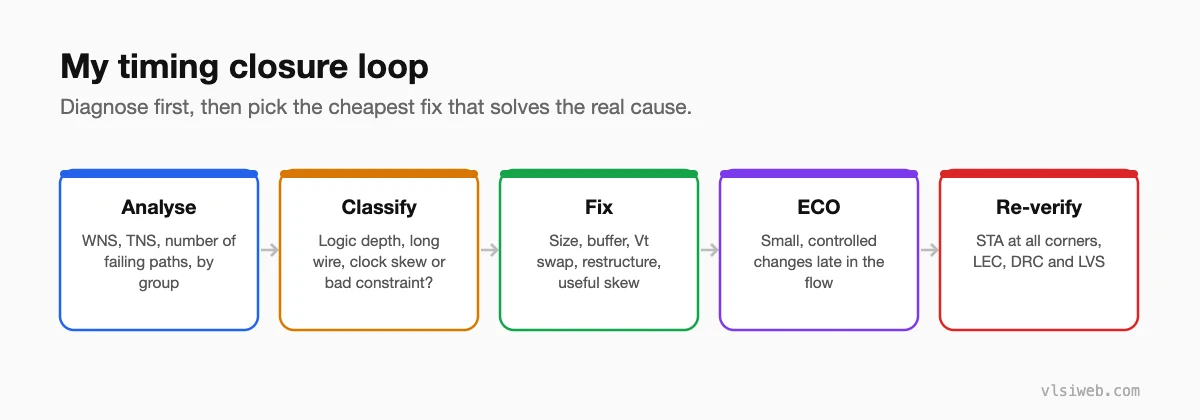
Part 1: The loop
Part 2: Reading the timing reports
- WNS (worst negative slack) tells you how bad the worst path is; TNS (total negative slack) and the number of failing endpoints tell you how widespread the problem is.
- Group failures by start and end points: many failures between two blocks usually point to a floorplan or constraint issue, not individual paths.
- For each bad path, check where the delay is: cell delay (logic depth), wire delay (distance), clock (skew, latency) or the constraint itself.
Part 3: Fixing setup violations
| Fix | When it helps | Cost |
|---|---|---|
| Upsize cells | Weak drivers on long or high-fan-out nets | Area, power, input load |
| Lower-Vt swap | Critical paths that need a few picoseconds | Leakage |
| Buffer insertion / repeaters | Long wires | Area, power |
| Move cells closer | Spread-out critical paths | May disturb other paths |
| Logic restructuring | Deep logic, late-arriving signals | Tool effort or RTL change |
| Useful skew | Path with slack on the neighbouring stage | Must keep hold and other paths clean |
| Pipeline or change RTL | Logic simply too deep for the clock | Latency, design change |
Part 4: Fixing hold violations
- Insert delay cells or buffers on the short path, near the capture flop.
- Downsize or use higher-Vt cells on the short path.
- Fix at the corner where hold is worst (usually the fast corner) and check that the change doesn’t create setup violations at the slow corner.
- Large hold violations often mean a clock problem (big skew) rather than a data path problem.
Part 5: ECOs
An engineering change order is a small change to a design that’s already placed and routed, made without re-running the whole flow.
| Type | Example |
|---|---|
| Timing ECO | Resize or buffer a handful of cells to fix late violations |
| Functional ECO | A logic bug found late: change a few gates to match corrected RTL |
| Metal-only ECO | After masks for base layers are made: use pre-placed spare cells and change only metal layers |
Every ECO must be followed by equivalence checking (for functional ECOs), STA at all corners, and DRC and LVS. Spare cells sprinkled across the design during placement make metal-only ECOs possible.
Part 6: Habits that speed up closure
- Check constraints first; a wrong clock or missing false path wastes days.
- Fix the biggest structural problems early (floorplan, logic depth) and leave fine-tuning to the end.
- Track WNS and TNS run to run; a sudden change usually has a single cause.
- Leave margin at early stages, because routing and SI will take some of it.
Practise this on VLSI Forge
I built VLSI Forge so you can write RTL in your browser, run it on a real simulator and check every signal in the waveform. Free, nothing to install.
Physical Design problems · Static Timing Analysis problems
Previous in my physical design series: Parasitics and crosstalk. Next: Sign-off timing and MCMM.
FAQ
What is timing closure?
The process of making every timing path meet setup and hold requirements at all sign-off corners and modes.
How do you fix a setup violation in physical design?
Upsize or swap to faster cells, buffer long wires, move cells closer, restructure logic, use useful skew, or change the RTL if the logic is too deep.
How do you fix a hold violation?
Add delay on the short data path with buffers or delay cells, or slower cells, while checking setup at the slow corners.
What is a metal-only ECO?
A design change made using only metal layers, typically by wiring in pre-placed spare cells, so base-layer masks don’t need to be remade.
