In digital circuit design, setup and hold time violations are big problems. They can really hurt how well our systems work. These timing rules make sure data is captured right by flip-flops, so our circuits work as planned.
Understanding setup and hold time helps us find and fix these timing issues. This makes our digital designs work better.
Setup time is how long data needs to be stable before the clock edge. Hold time is how long it must stay stable after the clock edge. If these times are not met, it can cause problems like metastability.
Metastability makes flip-flops unsure, leading to data errors and system crashes. It’s very important to fix these timing problems to keep our digital circuits running smoothly.
We use special tools and methods to find the causes of these timing issues. This includes things like clock-to-q delays, path imbalances, or wrong buffer use. With this knowledge, we can fix the problems.
We might use things like clock skew optimization, smart buffer placement, or balancing path delays. These steps help solve the timing problems and get our designs working right.
Table of Contents
Understanding Setup and Hold Time Basics
In digital circuit design, setup and hold time are key. They define when data must be stable for a clock edge to capture it. Knowing these basics is vital for our circuits to work well.
Definition of Setup Time Requirements
The setup time tells us how long data must be ready before the clock edge. This lets circuits process the data correctly. Following setup time rules helps avoid big problems with data stability.
Critical Hold Time Parameters
The hold time is just as important. It says how long data must stay stable after the clock edge. This ensures data is safely stored without issues. Ignoring hold time can cause system failures.
Impact on Digital Circuit Performance
Managing setup and hold time is essential for digital circuits to work right. Breaking these rules can lead to data errors and system crashes. Making sure our circuits meet these timing rules is key to their success.
Common Causes of Setup and Hold Violations
In digital circuit design, timing is key. Knowing why setup and hold time violations happen is vital for our systems’ reliability. Let’s look at the main reasons for these timing issues.
Clock skew is a big problem. When the clock signal travels at different speeds in the circuit, it can cause violations. This is especially true in complex designs with long paths and many clock domains.
Excessive propagation delay is another issue. If a signal takes too long to travel, timing problems arise. High fan-out, long wires, or complex logic gates can make this worse.
Signal integrity issues also play a role. Noise, crosstalk, and reflections can mess up the signal. This makes it hard for the circuit to read the data correctly.
The complexity of the logic is another factor. Complex paths with many gates and branches can cause unpredictable delays. These delays can lead to timing problems that are hard to fix.
By knowing these common causes, designers can tackle these issues early. This ensures their digital circuits work well and efficiently.

| Cause | Description | Impact on Timing |
|---|---|---|
| Clock Skew | Uneven propagation of the clock signal across the circuit | Leads to setup and hold time violations |
| Propagation Delay | Excessive time for a signal to travel from one point to another | Causes setup and hold time issues |
| Signal Integrity | Noise, crosstalk, and reflections that distort the signal shape | Introduces uncertainty in timing parameters |
| Logic Complexity | Intricate logic paths with multiple gates and branches | Leads to unpredictable delays and timing problems |
Tools and Methods for Timing Violation Detection
Finding and fixing setup and hold time violations is key for digital circuits to work well. We have many tools and methods to help with this. Let’s look at the main ways engineers find timing problems in their designs.
Static Timing Analysis Tools
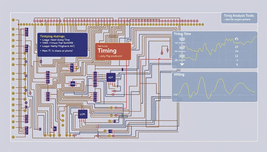
Static timing analysis (STA) tools are essential for checking timing. They use software to look at the circuit’s design and timing rules. This helps find potential timing issues.
STA tools show us important timing paths and how much time we have. They also give detailed reports. These reports help us improve our designs.
Dynamic Verification Techniques
STA tools are great for static analysis, but we also use dynamic verification. This involves simulating how the circuit works under different conditions. We look at things like temperature, voltage, and how the circuit changes.
By doing simulations, we see how the circuit really behaves. This helps us find any timing violations that might not show up in STA reports.
Waveform Analysis Methods
Waveform analysis is another important tool. It lets us look at the circuit’s timing waveforms with an oscilloscope or other tools. This way, we can see how signals interact.
Looking at waveforms helps us spot timing problems that might not be clear from STA reports alone.
Using STA tools, dynamic verification, and waveform analysis together helps us understand our circuit’s timing. This way, we can fix any setup or hold time violations. This approach makes sure our digital designs work well and reliably.
Setup and Hold Violation in PD
In the world of physical design (PD), setup and hold time violations are big challenges. They happen during the place and route stage. These timing issues make it hard to reach timing closure, a key goal in PD optimization.
Setup and hold time violations happen when input signals don’t meet timing specs. This can cause data to be sampled wrong, leading to errors and performance drops. In PD, we try to balance timing across the whole design.
Physical placement and routing of components often cause these violations. As we place and connect design elements, delays and skews can create timing problems. Finding the right balance between design, placement, and timing is a complex, iterative process.
To tackle these timing issues, we use various PD optimization techniques. Tools for static timing analysis help spot and measure violations. Dynamic verification, like waveform analysis, helps us understand timing better, guiding our adjustments.
By understanding setup and hold time management in PD, we can make sure our designs work well. This leads to successful timing closure and a solid PD implementation.

Best Practices for Timing Closure
Mastering timing closure is key to achieving top circuit performance. Our guide covers the best ways to fix setup and hold time issues.
Clock Skew Optimization
Clock skew affects timing closure by causing clock signal delays. Optimizing the clock tree synthesis helps reduce skew. This ensures our circuits work well within timing limits.
Buffer Insertion Strategies
Using buffers strategically is vital for timing management. By placing buffers in key spots, we can tackle long signal paths. This boosts signal quality and improves timing closure.
Path Delay Balancing
For the best timing closure, we need to balance path delays. Analyzing critical paths and adjusting delays helps. This spreads out slack, reducing violation risks and enhancing system reliability.

