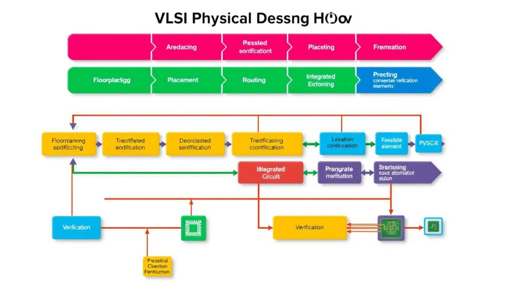
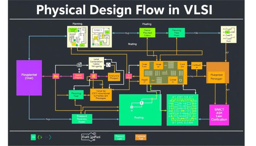
Physical design is key in the VLSI design flow. It turns the synthesized netlist and design rules into a layout that can be made. This process includes steps like partitioning, floorplanning, and placement.
It also involves clock tree synthesis, routing, and verification. The main aim is to reduce wire length, chip area, and power use. It must also meet strict timing needs.
Modern VLSI chips have over 50 billion transistors. This shows how crucial efficient physical design is. It helps create advanced integrated circuits.
By carefully following each step, engineers can make these systems work better. They become more efficient, powerful, and reliable. This is true for many fields, like data centers, telecommunications, automotive, and consumer electronics.
The need for skilled physical design engineers is growing. This highlights the vital role of this field in the VLSI design world.
Table of Contents
Understanding Physical Design in VLSI Manufacturing
Physical design in VLSI manufacturing is key. It turns logical circuits into real layouts. This can be done through full-custom or semi-custom designs.
Full-custom design means making everything from scratch, which is perfect but takes a lot of time and resources. Semi-custom design uses pre-made parts, saving time but might not be as optimal. The choice depends on how fast you need the product and how many you plan to make.
The goal of physical design in VLSI is to create chips that work well, use little power, and fit within manufacturing limits. It involves combining millions or billions of transistors into one chip. The design aims to optimize timing, performance, power use, and area.
The VLSI design flow makes the process consistent and easier for teams to work together. It includes stages like writing the design, making the layout, and checking the final product. This ensures the chip meets all the necessary standards.
Designing chips in VLSI comes with challenges like complexity, scaling, power, and time. To overcome these, advanced tools are used. These tools help with everything from placing components to checking the final design.
| Metric | Impact on Physical Design |
|---|---|
| Performance | Long routes may introduce significantly longer signal delays, impacting circuit performance. |
| Area | Placing connected modules far apart can lead to larger and slower chips. |
| Reliability | A large number of vias may significantly decrease circuit reliability. |
| Power | Transistors with smaller gate lengths may achieve greater switching speeds but at the cost of higher leakage current. |
| Yield | Wires routed too close together can result in decreased yield due to electrical shorts during manufacturing. |

In summary, physical design in VLSI manufacturing is vital. It transforms logical circuits into real layouts. The choice between full-custom and semi-custom designs depends on several factors. The design flow includes many stages to ensure the chip works well, uses little power, and is manufacturable.
PD in VLSI Flow: From Netlist to Layout
The physical design (PD) flow in VLSI engineering is key. It turns the abstract gate-level netlist into a real, manufacturable layout. This journey starts with the gate-level netlist, the base for all design phases.
Gate-Level Netlist Creation
The gate-level netlist comes from synthesis. It turns the RTL design into a network of logic gates. This netlist is what the physical design team uses to start the layout process.
Design Constraints and Requirements
Design constraints and requirements guide the physical design. These include timing, area, and power specs. They make sure the layout meets performance, power, and area targets, and follows foundry rules.
Layout Generation Process
The layout generation process has several steps. These are partitioning, floorplanning, placement, clock tree synthesis, and routing. Each step helps turn the netlist into a real layout that meets all design and foundry rules.
- Partitioning: The design is split into smaller blocks for better layout and easier implementation.
- Floorplanning: The blocks are placed on the chip to reduce area and delay.
- Placement: Standard cells are placed on the die for timing, congestion, and power optimization.
- Clock Tree Synthesis (CTS): Clock signals are distributed to sequential elements for uniform timing and less skew.
- Routing: Blocks are connected using metal and vias to meet timing and reduce wire length.
The physical design flow is an iterative process. It involves many rounds of optimization and verification. This ensures the final layout meets all design and foundry rules.
Essential Components of Physical Design Implementation
The physical design implementation in VLSI is key. It turns a circuit’s logical design into a real semiconductor chip. This process includes several important parts that work together to make a chip that can be made and works well. Let’s look at these main parts:
- Floorplanning: This first step decides the size and where things go in the chip’s core area. Good floorplanning helps use the silicon area well and makes routing easier.
- Placement: Placement puts the standard cells, which are the basic parts of the design, in the core area. It’s important for meeting timing and power needs.
- Routing: Routing connects the placed standard cells and blocks. It uses smart algorithms to keep signals clear and avoid congestion.
- Clock Tree Synthesis (CTS): CTS makes sure the clock signal reaches all parts of the chip evenly. This helps everything work together in sync.
- Physical Verification: The last step checks the design. It makes sure the layout can be made and that it works as planned.
These parts work together to make a chip layout that meets all needs. They are key to making VLSI designs work.

The physical design flow in VLSI is a detailed process. Each step is important for turning a design into a real chip. By knowing and using these core parts, VLSI designers can bring their ideas to life.
Placement and Optimization Techniques
Physical design in VLSI manufacturing is complex. It involves many techniques to meet performance, power, and area needs. Placement and optimization are key parts of this process.
Standard Cell Placement
Standard cell placement puts individual cells in the chip’s core area. The goal is to optimize for area, timing, and power. Techniques like buffer insertion and gate resizing are used to meet design constraints.
Timing-Driven Placement
Timing-driven placement focuses on meeting timing needs. It places cells to reduce critical path delays. This ensures the design meets its performance goals. Techniques like useful skew are used.
Congestion Management
Congestion management is crucial to avoid routing bottlenecks. It ensures enough space for interconnects. Strategies for high- and medium-utilization designs are used to prevent hotspots.
These techniques work together to create an optimal cell arrangement. By using standard cell placement, timing-driven placement, and congestion management, designers meet their optimization goals for VLSI designs.
| Technique | Description | Key Considerations |
|---|---|---|
| Standard Cell Placement | Positioning standard cells within the chip’s core area | Optimizing for area, timing, and power |
| Timing-Driven Placement | Positioning cells to minimize critical path delays | Meeting timing constraints, utilizing techniques like useful skew |
| Congestion Management | Avoiding routing bottlenecks and ensuring sufficient space for interconnects | Minimizing global and local congestion to prevent hotspots |
Clock Tree Synthesis and Routing Strategies
Clock tree synthesis (CTS) is key in physical design. It helps spread clock signals across the chip with little skew. This is vital for all parts of the chip to work in sync, like registers and SRAMs.
The CTS process makes a balanced tree to send the clock signal. This aims to cut down on clock skew, which affects timing and performance. Global and detailed routing help with this by managing wire lengths and signal integrity.
Advanced routing methods, like H-Tree and X-Tree, aim to evenly distribute the clock signal. They consider wire length and capacitance to make the clock network better. Good CTS and routing are essential for the chip’s performance and timing.
Source Links
- Steps In VLSI Physical Design Flow
- VLSI: Physical Design (PD P1) — Introduction to PD
- Physical Design Flow – Maven Silicon
- what is physical design
- The Definite Guide of Physical Design Flow In VLSI
- VLSI Physical Design Flow
- VLSI: Physical Design (PD P4) — Sanity checks in PD
- Physical Design Flow in details | ASIC Design Flow – Team VLSI
- Understanding the Importance of Prerequisites in the VLSI Physical Design Stage
- Physical Design Flow in VLSI
- Placement Optimization in VLSI Physical Design
- Placement & Optimization – SignOff Semiconductors
- Ultimate Guide: Clock Tree Synthesis – AnySilicon
- Clock Tree routing Algorithms

