In the world of chip design and semiconductor layout, area optimization is key. As integrated circuits (ICs) grow, making them smaller while keeping them fast and functional is crucial. We’ll look at how to use space wisely in these complex systems, making them cheaper and more energy-efficient.
The chip design process is complex, and area optimization is a big part of it. By using VLSI optimization strategies, we can make ICs smaller without losing their performance. This makes chips cheaper to make and use less power and stay cool.
In this article, we’ll explore the basics of semiconductor layout and the main ways to optimize area. We’ll see how hierarchical planning, cell placement, and routing help designers make chips better and cheaper. These methods are key to improving chip performance and cost.
Table of Contents
Understanding the Fundamentals of Physical Design Area Optimization
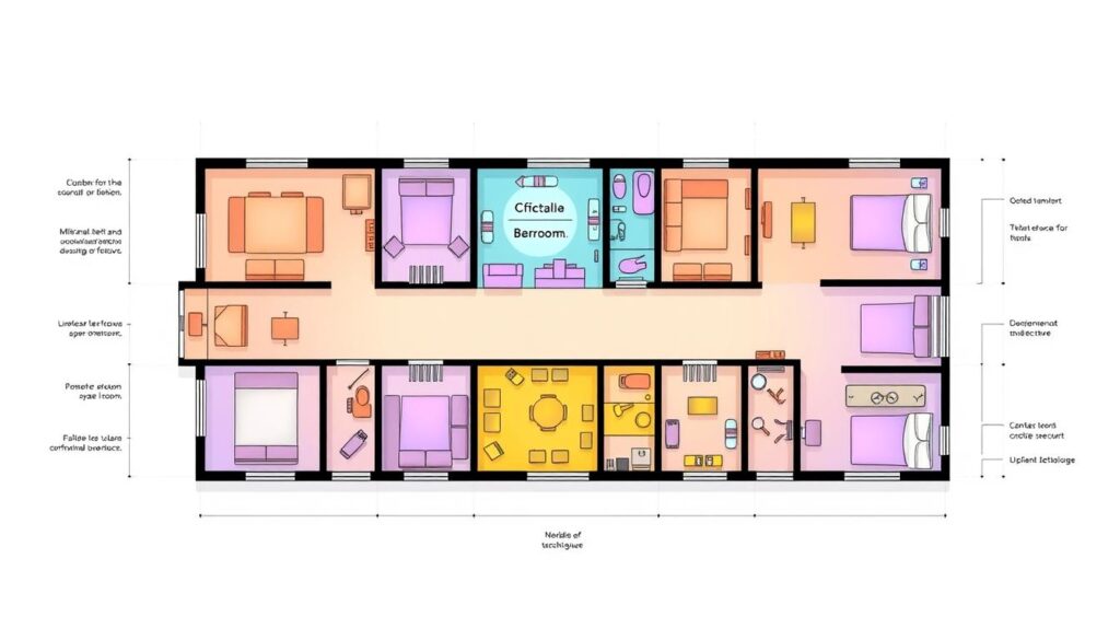
In chip design, making the physical layout better is key. This means using techniques to make the chip floorplan, standard cell placement, interconnect optimization, and power grid design more efficient.
Key Components of Physical Design Layout
The layout of a chip includes several important parts:
- Chip floorplan: The arrangement of different blocks in the chip
- Standard cell placement: Placing logic gates and components strategically
- Interconnect optimization: Routing electrical connections efficiently
- Power grid design: Creating a network for power delivery
Impact of Area Optimization on Chip Performance
Good area optimization can greatly improve a chip’s performance. It helps reduce delays, improve signal quality, and save power. These benefits lead to faster chips, less power use, and better reliability.
Basic Principles of Space Utilization
The area optimization process is based on key principles:
- Density maximization: Fitting components closely to use less space
- Aspect ratio management: Keeping the chip’s length and width in balance
- Hierarchy and modularity: Using design hierarchies and modules for better scalability and reuse
- Routing efficiency: Making the layout and interconnects less congested for better signal quality
By understanding and applying these principles, designers can create high-performance, efficient chips. These chips meet the needs of today’s computing and electronics.
Area Optimization in PD: Essential Methods and Strategies
In the world of physical design (PD), making the most of space is key. We’ll look at the main ways to cut down chip area without losing functionality. These include cell sizing, gate clustering, buffer insertion, and reducing wire lengths. These steps are vital for using every inch of the silicon die efficiently.
Cell sizing is a big part of this. It means changing the size of cells to find the best mix of area, power, and speed. By adjusting cell sizes, we can shrink the chip area while keeping it fully functional.
Gate clustering is another smart move. It groups related gates together to cut down on wire complexity. This way, we can use space better, making the layout more compact and efficient.
Adding buffers is also important for saving space. Buffers keep signals strong and clear, especially over long distances. By placing buffers wisely, we can keep signals reliable and use less area.
Finally, wire length reduction is a must for smaller chips. By smartly routing wires, we can make the layout more compact and signals stronger. This helps us use every bit of silicon space well.
By using these key methods, designers can optimize chip area effectively. They balance a small layout with top-notch circuit performance. These techniques are essential for making high-performance, space-saving chips for today’s electronics.
Floor Planning Techniques for Efficient Space Management
In the world of integrated circuit design, floor planning is key to using space well. Designers use advanced techniques to manage chip space, making designs more efficient and less wasteful. Let’s look at some main methods that help achieve this goal.
Hierarchical Floor Planning Approaches
The hierarchical approach is a top floor planning strategy. It divides the chip into smaller sections or hierarchies. This makes it easier to optimize each part, like macro placement and IP block integration.
By focusing on these parts, designers can make the chip more efficient. This leads to a better overall design.
Placement-Aware Floor Planning
Placement-aware floor planning is also crucial. It considers where components should go early on. This ensures they are placed to save space.
Techniques like adjusting the aspect ratio help too. They find the best balance between the chip’s width and height. This makes the design more compact and efficient.
Aspect Ratio Considerations
The aspect ratio is vital in floor planning. It’s the chip’s width to height ratio. Adjusting this ratio helps make the chip layout more compact and efficient.
Designers analyze the design’s needs to find the best aspect ratio. This maximizes space without losing performance.
Using these advanced floor planning techniques is essential. They include hierarchical approaches, placement-aware strategies, and aspect ratio adjustments. These methods help designers optimize chip area, leading to more efficient designs.

Cell Placement and Optimization Techniques
Optimizing cell placement on a chip is key to reducing area usage. We’ll look at important techniques like legalization, detailed placement, and more. These methods help in achieving a better chip design.
Legalization makes sure cells follow design rules. It ensures cells don’t overlap and stay within their areas. This step is crucial for further optimization.
Detailed placement refines the initial placement. It aims to cut wirelength, reduce congestion, and improve timing. Advanced algorithms are used to place cells carefully, balancing design goals.
Congestion-driven placement tackles congestion hotspots. It places cells to reduce congestion, making routing easier and shrinking chip area.
Timing-driven placement focuses on critical timing paths. It ensures cells are placed for optimal circuit performance. This involves balancing area, power, and timing carefully.
Using these techniques together is vital for a high-performing chip. They help designers reduce area while keeping the chip functional and efficient.

Routing Strategies for Minimizing Area Usage
In the world of Physical Design, making the routing process more efficient is key. This helps in using less area on integrated circuits. We’ll look at ways to do this, like using multiple layers for routing, reducing vias, and making the most of routing tracks.
Multi-Layer Routing Optimization
Today’s chips use many metal layers for complex connections. By planning routes across these layers, we can use less area. This means we need to optimize both global and detailed routing to use metal layers well.
Via Minimization Techniques
Vias connect metal layers and can affect area usage. With techniques like via stapling, we can cut down on vias. This makes the routing layout more efficient and saves area.
Track Utilization Methods
Using routing tracks efficiently is also important. By applying track compaction algorithms, we can make the most of available tracks. This results in a more compact and efficient routing layout.

