


The short answer: Combinational logic has no memory: its outputs depend only on its current inputs. In Verilog you write it with assign statements or with always @(*) blocks using blocking assignments. The golden rule is that every output must be assigned on every path through the block; otherwise synthesis infers a latch. Avoid combinational feedback loops, and keep logic depth in mind because it sets your clock frequency.
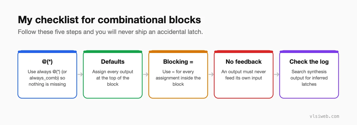
Most of a chip’s logic is combinational: decoders, multiplexers, adders, comparators, next-state logic. Writing it is easy; writing it so it never creates a latch or a loop takes a little discipline. Here’s the checklist I use and a set of examples worth knowing by heart.
- The checklist
- Example: a small ALU
- Example: priority encoder
- Example: decoder and mux
- Latches: how they sneak in
- Combinational loops
- Thinking about timing
Table of Contents
Part 1: The checklist
Part 2: Example: a small ALU
module alu #(parameter W = 8) (
  input  wire [W-1:0] a, b,
  input  wire [2:0]   op,
  output reg  [W-1:0] y,
  output wire         zero
);
  localparam ADD = 3'd0, SUB = 3'd1, AND_ = 3'd2,
             OR_ = 3'd3, XOR_ = 3'd4, SLT = 3'd5;

  always @(*) begin
    y = {W{1'b0}};                    // default
    case (op)
      ADD:  y = a + b;
      SUB:  y = a - b;
      AND_: y = a & b;
      OR_:  y = a | b;
      XOR_: y = a ^ b;
      SLT:  y = ($signed(a) < $signed(b)) ? 1 : 0;
      default: y = {W{1'b0}};
    endcase
  end

  assign zero = (y == {W{1'b0}});
endmodule
Part 3: Example: priority encoder
// index of the highest set bit; valid = 0 when no bit is set
always @(*) begin
  idx   = 3'd0;
  valid = 1'b0;
  for (i = 0; i < 8; i = i + 1)
    if (req[i]) begin
      idx   = i[2:0];      // later (higher) bits overwrite earlier ones
      valid = 1'b1;
    end
end
Because the loop runs from bit 0 upwards and later assignments win, the highest set bit has priority. This loop pattern scales to any width.
Part 4: Example: decoder and mux
// 3-to-8 one-hot decoder
assign onehot = en ? (8'b1 << sel) : 8'b0;

// parameterised N:1 mux using an array select
assign y = data[sel*W +: W];
Part 5: Latches: how they sneak in
// BAD: no else, so y must hold its value when en = 0 -> latch
always @(*)
  if (en) y = d;

// GOOD
always @(*) begin
  y = 1'b0;
  if (en) y = d;
end
Latches are hard to time, hard to test and almost never intended in ASIC RTL. Synthesis tools report every inferred latch; search the log for “latch” after every run.
Part 6: Combinational loops
If an output feeds back into its own logic without a flip-flop in the way (assign a = b & c; assign c = a | d;), you’ve built a loop. It can oscillate or latch, simulators may hang, and STA can’t time it. Break every loop with a register.
Part 7: Thinking about timing
- Every level of logic adds delay. A long if-else chain or a wide adder sets the minimum clock period.
- Wide comparators and adders are fine; tools build fast versions. Deeply nested decisions are the usual problem.
- If a path is too long, split it with a pipeline register. See the RTL design interview questions for pipelining examples.
Practise this on VLSI Forge
I built VLSI Forge so you can write RTL in your browser, run it on a real simulator and check every signal in the waveform. Free, nothing to install.
RTL Design problems · Daily challenge
Previous in my Verilog series: if, case and loops. Next: Flip-flops, latches, registers and counters.
FAQ
How do I write combinational logic in Verilog?
With assign statements for simple expressions, or always @(*) blocks with blocking assignments for anything that needs if or case. Assign every output on every path.
Why does my combinational always block create a latch?
Some output isn’t assigned on some path. Add default assignments at the top or complete every if and case.
Should I use = or <= in always @(*)?
Blocking (=). Non-blocking in combinational logic adds unnecessary delta cycles and can confuse readers.
What is a combinational loop?
A path where a signal feeds back into its own logic without passing through a flip-flop. Avoid them in synchronous design.
