

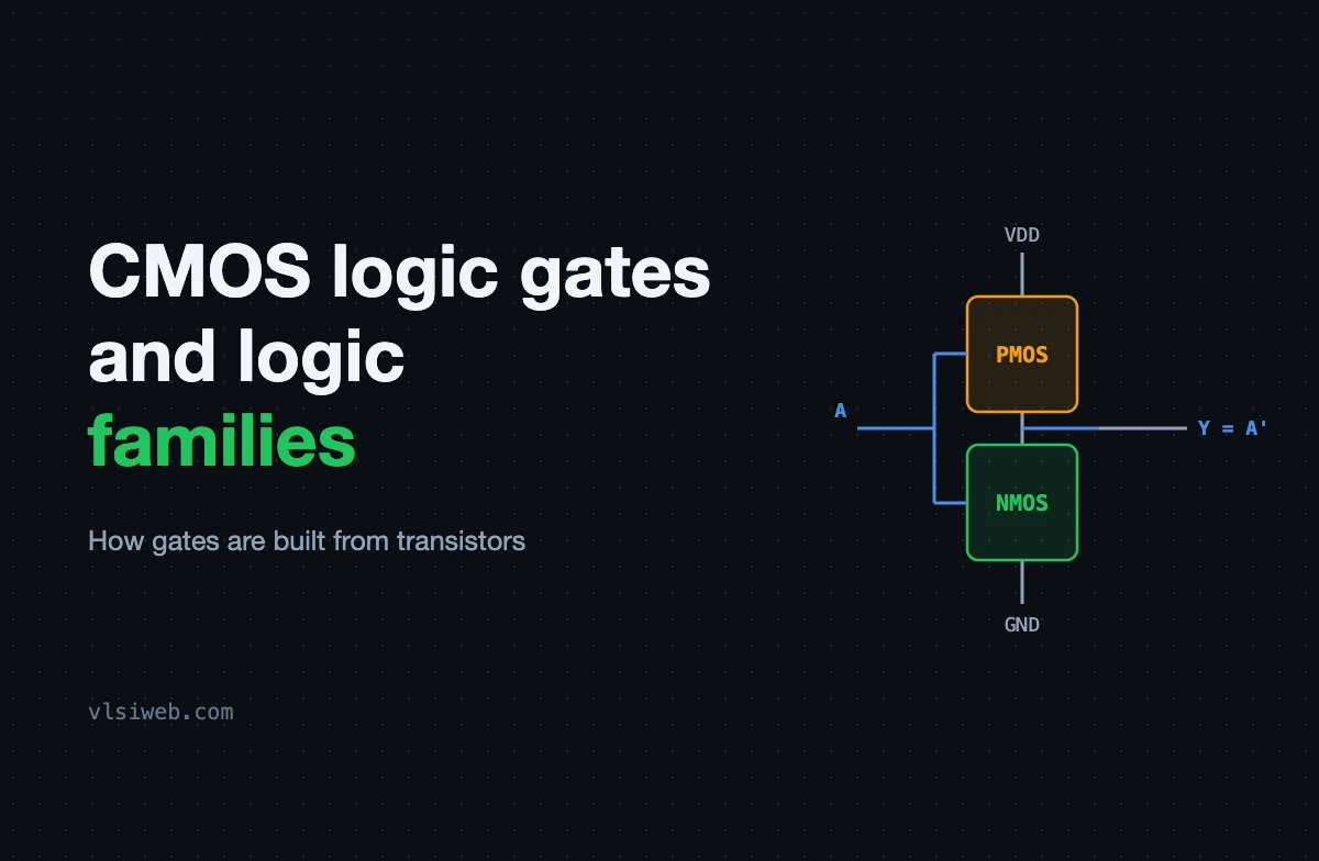
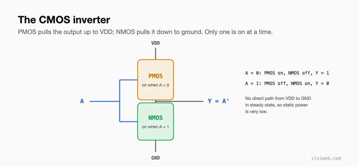
The short answer: almost every digital chip today is built in CMOS, where each gate has a pull-up network of PMOS transistors and a pull-down network of NMOS transistors. For any input, only one network conducts, so the output is driven cleanly to VDD or ground and very little static power is used. Older logic families such as TTL and ECL are mostly of historical interest now, apart from niche uses.
Understanding how gates are built from transistors explains a lot: why NAND gates are preferred over NOR, why delay depends on load, and where power goes. This post combines my older posts on transistor-level gates and logic families.
- The CMOS inverter
- NAND and NOR at transistor level
- Where power goes in CMOS
- Logic families compared
- Why this matters for RTL engineers
Table of Contents
Part 1: The CMOS inverter
Part 2: NAND and NOR at transistor level
- NAND: two NMOS transistors in series pull the output low only when both inputs are 1; two PMOS transistors in parallel pull it high when either input is 0.
- NOR: two NMOS in parallel and two PMOS in series.
- Because PMOS transistors are weaker than NMOS, putting PMOS in series (as NOR does) makes the gate slower or bigger. That is a big reason NAND-based logic is preferred.
Part 3: Where power goes in CMOS
- Dynamic power: charging and discharging load capacitance each time a node switches, roughly proportional to C × V² × f × activity.
- Short-circuit power: a brief current while both networks are partly on during a transition.
- Leakage power: small currents that flow even when nothing switches, which grow as transistors shrink.
This is why clock gating (cutting activity) and lowering voltage are the most effective power-saving techniques.
Part 4: Logic families compared
| Family | Built from | Notes |
|---|---|---|
| CMOS | PMOS and NMOS transistors | Dominant today: low static power, high density |
| TTL | Bipolar transistors | Classic 74-series chips; mostly legacy now |
| ECL | Bipolar, non-saturating | Very fast but power-hungry; niche high-speed uses |
| BiCMOS | Bipolar plus CMOS | Mixes speed and density; used in some analog and RF chips |
Part 5: Why this matters for RTL engineers
You will rarely draw transistors, but this knowledge explains synthesis and timing results: why a long chain of logic is slow, why high fan-out nets need buffering, and why the tools prefer certain gates. It also helps a lot in physical design and STA interviews.
Practise this on VLSI Forge
I built VLSI Forge so you can write RTL in your browser, run it on a real simulator and check every signal in the waveform. Free, nothing to install.
Digital logic problems · STA problems
FAQ
Why is CMOS so widely used?
It uses very little static power, scales well to small transistors and packs many gates into a small area.
Why is NAND preferred over NOR in CMOS?
NOR puts PMOS transistors in series, and PMOS is weaker than NMOS, so NOR gates are slower or need bigger transistors.
How many transistors does a CMOS NAND gate need?
Four for a 2-input NAND: two PMOS and two NMOS.
Is TTL still used?
Mostly in older systems and hobby electronics. New chip designs use CMOS.
