


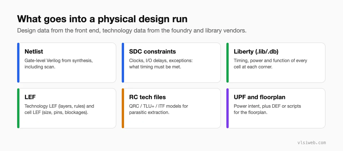
The short answer: A physical design run needs design data and technology data. Design data comes from the front end: the gate-level netlist, SDC timing constraints, UPF power intent and sometimes a floorplan DEF. Technology data comes from the foundry’s process design kit (PDK) and library vendors: Liberty timing libraries, technology and cell LEF, RC extraction models, design rule decks and device models. EDA tools combine all of this into one database, and most of PD is making sure these inputs are complete and consistent.
A surprising number of PD problems turn out to be input problems: a missing corner library, a wrong SDC, a stale LEF. Knowing what each file is for makes those problems much easier to spot. This post combines my older posts on process design kits and EDA tools in PD.
- The inputs
- What’s in a PDK
- Liberty and LEF in one sentence each
- The tools
- Sanity checks before you start
Table of Contents
Part 1: The inputs
Part 2: What’s in a PDK
| Item | Used for |
|---|---|
| Device models (SPICE) | Circuit simulation and library characterisation |
| Design rules (DRC deck) | Physical verification |
| LVS and extraction rule decks | Layout vs schematic, parasitic extraction |
| Technology files | Layer stack, widths, spacings, vias for P&R |
| Standard cell and I/O libraries | Usually from the foundry or a library vendor |
| Memory compilers and IP | SRAMs, PLLs, I/Os and other hard blocks |
PDKs are under strict NDA and versioned carefully; mixing versions between tools is a classic source of sign-off mismatches.
Part 3: Liberty and LEF in one sentence each
- Liberty (.lib) tells the tools how each cell behaves: delay and transition tables versus input slew and output load, setup and hold, power and leakage, at one process-voltage-temperature corner per file.
- LEF tells the tools what each cell looks like physically: its size, pin shapes and blockages (cell LEF), and the metal layers, vias and routing rules of the technology (tech LEF).
The database format DEF describes a placed and routed design (or just a floorplan) and is how designs move between tools.
Part 4: The tools
| Task | Commercial examples | Open-source |
|---|---|---|
| Place and route | Cadence Innovus, Synopsys Fusion Compiler / IC Compiler II | OpenROAD |
| Static timing | Synopsys PrimeTime, Cadence Tempus | OpenSTA |
| Extraction | StarRC, Quantus | OpenRCX |
| IR drop / EM | Ansys RedHawk, Cadence Voltus | – |
| Physical verification | Siemens Calibre, Synopsys ICV, Cadence Pegasus | KLayout, Magic, Netgen |
| Formal equivalence | Formality, Conformal | Yosys-based flows |
If you’re learning PD without access to commercial tools, OpenROAD with an open PDK such as SkyWater 130 nm or GF180 lets you run the whole flow on a laptop.
Part 5: Sanity checks before you start
- Every cell in the netlist has a Liberty and LEF view.
- Libraries exist for every corner and mode you need to sign off.
- check_timing on the SDC reports no unconstrained endpoints or missing clocks.
- The netlist passes equivalence checking against the RTL.
- The tool versions match what the PDK supports.
Practise this on VLSI Forge
I built VLSI Forge so you can write RTL in your browser, run it on a real simulator and check every signal in the waveform. Free, nothing to install.
Physical Design problems · Static Timing Analysis problems
Previous in my physical design series: What is physical design?. Next: Floorplanning.
FAQ
What is a PDK?
A process design kit: the foundry’s package of device models, design rules, technology files and verification decks needed to design for a specific process.
What is the difference between LEF and Liberty?
LEF describes the physical shape and pins of cells and the technology layers; Liberty describes timing, power and function.
What is DEF?
Design Exchange Format: a text description of a floorplan or a placed and routed design, used to move data between tools.
Can I learn physical design with free tools?
Yes. OpenROAD with an open PDK like SkyWater 130 nm runs the full flow from netlist to GDSII.
