Hold time is an essential aspect of Static Timing Analysis (STA) that we must understand and optimize in our digital circuit designs. It plays a crucial role in ensuring reliable and efficient circuit operation. By maintaining a stable data signal for a specified amount of time after the clock event, we can prevent timing violations and errors.
In this article, we will dive into the concept of hold time and its significance in STA. We will explore how hold time impacts flip-flop behavior, synchronization of data, and the overall performance of digital circuits.
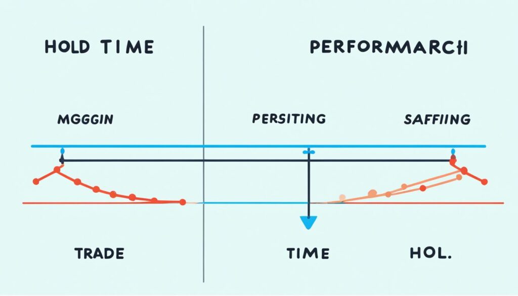
Additionally, we will discuss the importance of hold time margin and the trade-offs associated with optimizing this parameter. By balancing hold time margin with power, performance, and area requirements, we can achieve the desired balance in our circuit designs.
Join us as we unravel the complexities surrounding hold time in STA and discover how it can be effectively utilized to create reliable and efficient digital circuits.
Table of Contents
What is Hold Time?
Hold time is a crucial timing parameter in digital circuits, especially in the context of flip-flops and data capture. It refers to the minimum duration that the data input must remain stable after the clock edge to ensure accurate and reliable data capture in a flip-flop.
In simple terms, hold time defines the period during which the data must be held steady after the clock signal transitions. If the data changes before this hold time has elapsed, it can result in setup and hold violations, leading to incorrect circuit behavior and timing violations.
Hold time plays a vital role in achieving proper synchronization of data and preventing timing violations in digital circuits. By respecting the hold time requirement, designers can ensure that the data is reliably captured by the flip-flop and that the circuit operates as intended.
Understanding the Timing Violations
Timing violations occur when the hold time requirement is not met. There are two primary timing violations related to hold time:
- Setup violation: This violation occurs when the data input changes too close to the active edge of the clock signal, not allowing sufficient time for the data to stabilize before the clock transition. It can lead to unpredictable circuit behavior and unreliable data capture.
- Hold violation: A hold violation occurs when the data input changes before the required hold time has elapsed after the active edge of the clock signal. It can result in data corruption, unreliable circuit operation, and timing issues.
It is essential to mitigate these timing violations by designing circuits with appropriate hold time margins and by optimizing circuit parameters to ensure reliable data capture and proper synchronization.
How Hold Time is Impacted by Flip-Flops
Flip-flops, also known as bistable multivibrators, are widely used in digital circuits for data storage and synchronization. They have two stable states and allow for sequential circuit design. Hold time becomes critical in the context of flip-flops because it defines the duration for which the data input must remain stable after the clock transition to ensure accurate data storage.
Flip-flops typically have a setup time requirement, which indicates how long the data input must be stable before the clock event to ensure proper capture. Once the setup time has been met, the hold time requirement comes into play, determining how long the data input must remain stable after the clock transition.
Hold Time vs. Setup Time
| Parameter | Hold Time | Setup Time |
|---|---|---|
| Definition | The minimum time that the data input should remain stable after the active edge of the clock signal. | The minimum time that the data input should be stable before the active edge of the clock signal. |
| Violation Consequence | Timing violations and erroneous circuit behavior. | Timing violations and unpredictable circuit behavior. |
| Relationship | Hold time must be met after the setup time requirement has been satisfied. | Setup time must be met before the hold time requirement comes into effect. |
Understanding the relationship between hold time and setup time is crucial for precise circuit design and avoiding timing issues. By considering both parameters and implementing appropriate margins, designers can ensure reliable data capture, minimize timing violations, and achieve optimal circuit performance.
Importance of Hold Time Margin
The hold time margin plays a crucial role in digital circuit design, as it directly impacts the overall performance, power consumption, and area requirements of the circuit. By understanding and optimizing the hold time margin, designers can achieve the desired balance between these competing factors.
The hold time margin refers to the difference between the actual data arrival time and the required hold time in a digital circuit. A positive hold time margin indicates that the data meets the timing requirements, ensuring reliable circuit operation. Conversely, a negative margin indicates a hold violation, leading to timing errors and unreliable circuit behavior.
Optimizing the hold time margin is essential for achieving a stable and efficient digital circuit design. A larger hold time margin provides more cushion for data stability, reducing the chances of timing violations and improving overall circuit reliability. However, it’s important to note that an excessively large hold time margin may lead to performance degradation.
By finding the optimal hold time margin, designers can strike the right balance between power, performance, and area requirements. This balance ensures reliable circuit operation while maximizing efficiency and minimizing power consumption.
Here’s a summary of the key considerations related to hold time margin:
- Positive hold time margin: Indicates that the data meets the timing requirements
- Negative hold time margin: Indicates a hold violation and potential timing errors
- Larger hold time margin: Provides more cushion for data stability, improving circuit reliability
- Excessively large hold time margin: May lead to performance degradation
- Optimal hold time margin: Balances power, performance, and area requirements for efficient circuit design

Example Table: Hold Time Margin Comparison
| Hold Time Margin | Timing Violations | Power | Performance | Area |
|---|---|---|---|---|
| Large Positive Margin | Low | Optimal | High | Optimal |
| Small Positive Margin | Possible | Optimal | Optimal | Optimal |
| Negative Margin | High | High | Reduced | Increased |
This table provides a comparison of different hold time margin scenarios and their impact on timing violations, power consumption, performance, and area requirements. It highlights the trade-offs associated with hold time margin optimization to guide designers in making informed decisions during the digital circuit design process.
Trade-offs with Hold Time Margin
The hold time margin in a digital circuit can have trade-offs with power, performance, and area. When designing a digital circuit, setting the proper hold time margin is crucial for achieving optimal circuit performance while balancing power consumption and area requirements.
A larger hold time margin can improve overall performance by allowing for a higher clock frequency and reduced latency. By providing more time for the data signal to stabilize before the next clock event, a larger hold time margin helps to ensure reliable data capture in flip-flops and reduces the likelihood of timing violations.
However, it’s important to consider the potential impact on power consumption. A larger hold time margin can result in increased power consumption due to higher switching activity. The additional time for data stabilization can lead to more frequent state changes, resulting in increased power dissipation. Therefore, designers must carefully evaluate the power constraints of the circuit and balance the hold time margin against the desired performance gains.
Conversely, reducing the hold time margin can lead to certain benefits. With a smaller margin, it is possible to achieve improved performance, such as higher clock frequencies and reduced latency. This can be advantageous in applications where timing is critical, such as high-speed data processing. However, reducing the hold time margin too much may compromise circuit stability, leading to potential timing violations and erroneous circuit behavior.
Designers must take into account the specific power, performance, and area requirements of the digital circuit and find the optimal hold time margin that strikes the right balance. This involves careful trade-offs and considerations to ensure reliable circuit operation, efficient power consumption, and the desired performance levels.
Hold Time Margin Trade-offs Overview:
| Trade-Offs | Effects |
|---|---|
| Larger Hold Time Margin | – Improved performance – Increased power consumption |
| Smaller Hold Time Margin | – Potential for improved performance – Risk of circuit instability |

Conclusion
Hold time plays a crucial role in Static Timing Analysis (STA) when designing digital circuits. It ensures the proper synchronization of data and helps prevent timing violations, which can lead to errors in circuit operation. By understanding and optimizing hold time, we can achieve reliable circuit performance.
When designing digital circuits, it is important to balance the hold time margin with power, performance, and area requirements. This optimization process allows us to create efficient and reliable circuits that meet the desired specifications and performance targets.
Through careful analysis and optimization of hold time, we can strike the right balance between circuit stability and performance. By considering the power, performance, and area requirements, we can achieve the desired trade-offs and design digital circuits that are efficient and reliable.
In summary, hold time is a critical parameter that must be taken into account during the design process. By optimizing hold time, we can prevent timing violations, achieve reliable circuit performance, and create digital circuits that meet the desired specifications and performance targets.

