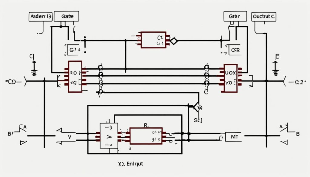
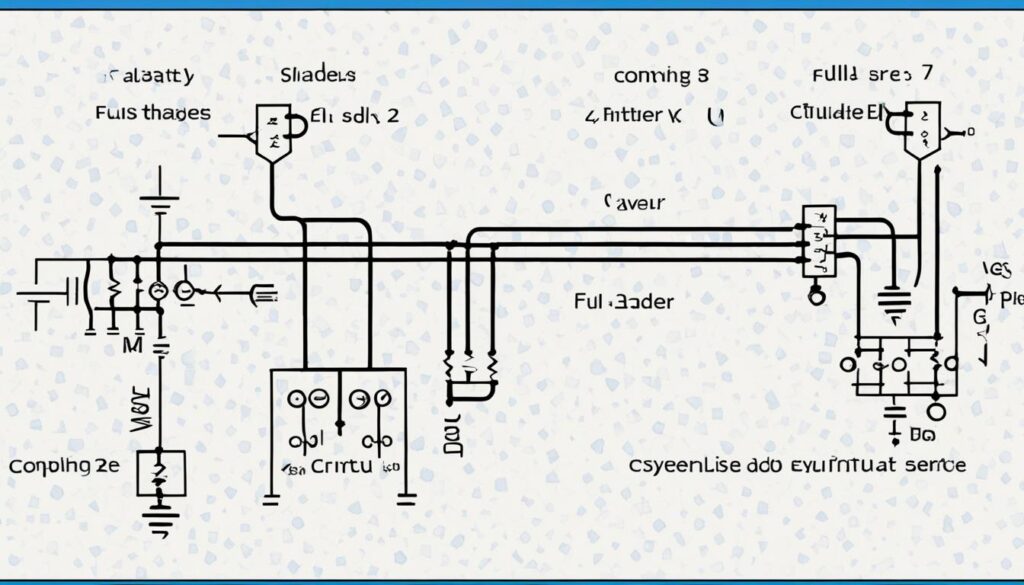
In the realm of digital circuits, two components that stand as fundamental pillars are the half adder and full adder. These devices are the backbone of binary addition, which is a critical operation within the field of computer arithmetic and overall computational tasks. Our understanding of these combinational logic circuits is crucial for the advancement of digital technology and the efficiency of modern computing systems.
A half adder’s role is straightforward yet indispensable; it adds two single-bit digits using an XOR gate for the sum and an AND gate for the carry. This simplicity is foundational, but as we expand into more complex operations, the full adder takes the stage, handling three 1-bit binary numbers and weaving through an intricate network of two XOR gates, two AND gates, and an OR gate to provide the sum and carry outputs.
We appreciate the ingenuity behind these devices, which are not only critical in the arithmetic logic units (ALUs) of computers but also underscore our ever-increasing capabilities in digital circuit design and implementation.
Table of Contents
Introduction to Digital Adders
As builders of the virtual landscapes that allow for intricate calculations and data processing, we understand the foundational role digital adders play in all forms of digital computation. These crucial components are more than mere bits of silicon; they are the embodiments of logic and arithmetic that power modern computing systems.
Definition of Half Adder and Full Adder
The definition of digital adders begins with understanding their simplest form: the half adder. A half adder takes two binary digits and combines them to produce a sum and a carry. Advanced by nature, a full adder escalates this operation by adding three binary digits, acknowledging a carry from a previous calculation, a testament to the relentless progression within the field of digital electronics.
Significance in Digital Computation
The significance of digital adders becomes apparent when we consider their ubiquitous role in enabling binary addition. Whether it’s in microprocessors, digital counters, or sophisticated algorithms, the functionality of both half and full adders serves as a critical pillar supporting the complex architecture of digital arithmetic operations. Their ability to relay and compile computations underpins the vast networks of data on which we’ve come to rely.
| Feature | Half Adder | Full Adder |
|---|---|---|
| Binary Digits Added | Two | Three |
| Outputs | Sum, Carry | Sum, Carry |
| Complexity | Basic | Advanced |
| Primary Use | Simple calculations | Complex arithmetic and sequential circuits |
| Building Backdrop | Foundational element for more complex adders | Facilitates multi-bit binary addition across broader computations |
The Operational Mechanics of Half Adders
Exploring the intricacies of operational mechanics within digital computation, we find ourselves closely examining half adders, indispensable units for arithmetic operations in digital circuits. The practicality of half adders lies in their ability to execute logical operations on two-single bit numbers, which is a foundational task in the realm of digital processing.
Central to the functionality of half adders is the XOR gate, which ingeniously calculates the sum of the two input digits without accounting for any carry from a previous operation. This elegant execution by the XOR gate is what predominantly shapes the sum output of a half adder.

Complementarily, the AND gate performs a pivotal role in the operational mechanics of the half adder by ascertaining the carry output. When both inputs are ‘1’, the AND gate asserts a carry, otherwise, the output remains null, indicating no carry is warranted.
Furthermore, the outputs, the sum, and the carry from the half adder, offer themselves as inputs for subsequent addition operations. This cascading ability is what enables half adders to act as fundamental building blocks within more complex digital circuits where multiple binary additions are necessary.
Delving into the operational mechanics of half adders, we are reminded of their crucial role and their seamless integration into larger computational architectures. Below, we outline the primary outputs of a half adder and elucidate their resulting functions:
| Input A | Input B | XOR Gate Output (Sum) | AND Gate Output (Carry) |
|---|---|---|---|
| 0 | 0 | 0 | 0 |
| 0 | 1 | 1 | 0 |
| 1 | 0 | 1 | 0 |
| 1 | 1 | 0 | 1 |
In summary, the elegant operational mechanics underpinning half adders facilitate the execution of basic addition in binary systems, heralding complex computational potential in broader digital technologies.
Half Adder and Full Adder: Key Differences and Uses
Understanding the nuances between half adders and full adders is crucial to appreciating their individual uses and the complexity each brings to digital circuits. Their distinct characteristics dictate the scope of their application and the transition processes within practical computing scenarios.
Comparing the Complexity and Application
The differences between half adders and full adders extend beyond their input and output configurations; they encompass the intrinsic complexity of their designs and their application in various computational tasks. For instance, half adders, with their simpler configuration, are adept for straightforward, single-digit binary addition. Conversely, their counterparts, full adders, address more complex scenarios where multi-bit arithmetic calculations are required, effectively exemplifying the sophistication of digital computation.

To provide a clearer perspective, the following table lays out the primary differences and uses of half adders and full adders within the realm of digital circuitry:
| Feature | Half Adder | Full Adder |
|---|---|---|
| Inputs | Two (A, B) | Three (A, B, Carry-in) |
| Outputs | Two (Sum, Carry) | Two (Sum, Carry-out) |
| Complexity | Lower (Only AND and XOR gates) | Higher (AND, XOR, and OR gates) |
| Uses | Simple addition | Extended addition, multi-bit binary addition |
| Application | Small scale digital operations | Comprehensive digital systems, CPUs |
Transition from Half Adders to Full Adders in Practical Circuits
In our experience, the transition from using half adders to integrating full adders in circuit design symbolizes an evolution in processing power and the ability to perform advanced computations. In simple designs, where additional complexity is unnecessary, a half adder suffices. However, as the demands for functionality increase, full adders become indispensable due to their ability to interact with aggregated binary data. This transition is a practical testament to the dynamic range of uses and applications that digital adders bring to technology advancements.
Breaking Down Full Adder Functionality and Design
In our analysis of digital systems, the full adder emerges as a cornerstone in the architecture of modern computing. Its functionality extends far beyond basic addition, offering an intricate example of design efficiency in digital logic. Let’s delve deeper into the workings of a full adder and its significance in computational electronics.
Comprehensive Analysis of a Full Adder’s Logic
The essence of the full adder’s functionality is to manage the arithmetic of three binary inputs: two primary operands and a carry from the preceding calculation stage. The digital dance of the logic gates is choreographed precisely, with XOR gates orchestrating the summing operation and AND gates determining the carry output—a high-stakes performance where precision is key for computational accuracy.
At a glance, the gracefully interlinked gates might seem daunting, but upon closer inspection, the design unfolds layers of logical sequences that beautifully converge to produce reliable results.
Implementing Full Adders in Digital Systems
The implementation of full adders is largely reliant on well-established Boolean algebra. Within the realm of calculators, computers, and advanced digital processors, these devices underscore the importance of robust logic and seamless integration for optimal performance. The incorporation of full adders in today’s digital systems underlines their pivotal role in computation and electronic design.
The table below showcases the critical relationship between input combinations and their corresponding output within a full adder’s circuitry:
| Input A | Input B | Carry In | Sum (Output) | Carry Out (Output) |
|---|---|---|---|---|
| 0 | 0 | 0 | 0 | 0 |
| 0 | 1 | 0 | 1 | 0 |
| 1 | 0 | 0 | 1 | 0 |
| 1 | 1 | 0 | 0 | 1 |
| 0 | 0 | 1 | 1 | 0 |
| 0 | 1 | 1 | 0 | 1 |
| 1 | 0 | 1 | 0 | 1 |
| 1 | 1 | 1 | 1 | 1 |
As we continue to push the boundaries of what’s possible in digital realms, the full adder serves as a reminder that complex functionality often arises from the intelligent interplay of fundamental components. Through deliberate design and careful implementation, these building blocks create the vast network of logic that powers our technological world.
Conclusion
In our exploration of digital circuit design, we’ve underscored the pivotal roles of half adders and full adders as foundational components. These integral units orchestrate the addition of binary numbers, a critical function that underpins the vast landscape of digital computation. Half adders adeptly manage the summing of two binary digits, presenting the springboard for basic computational tasks. In their stride, full adders escalate this capability by accommodating an additional binary digit, which enables the processing of extended arithmetic operations.
The intricacies in the design and functionality of these adders reveal a network of logic gates and circuits — from XOR to AND, and OR. These elements work in concert to translate discrete electrical impulses into meaningful data operations. This not only exemplifies the ingenuity embedded in their architecture but also the promise they hold in advancing computing efficiency.
As we draw this discussion to a conclusion, it’s evident that the principles and applications of half adders and full adders are not merely academic exercises but are instrumental in constructing complex digital systems. The proficiency in harnessing these devices is a testament to our continuous pursuit of technological advancement. A thorough understanding of these adders equips us with the tools to drive innovation in computing and remain at the forefront of the digital age.

