In the world of electronic systems, keeping signals clear and avoiding interference is key. Crosstalk and signal noise can really hurt how well devices work. We’ll look at ways to fix these problems, making sure our devices run smoothly.
We’ll talk about everything from basic ideas to advanced fixes. Engineers and designers use many strategies to improve signal quality and cut down on noise. Knowing where signal problems come from and how they affect circuits helps us find solutions.
Designing physical solutions, like using shields and grounding, is important. It helps keep signals separate and reduces crosstalk. We’ll also see how digital signal processing can help lower noise and make signals better.
Testing and measuring are also vital for signal quality. Using the right tests and tools helps us find and fix problems. This ensures our electronic systems work as well as they can.
Table of Contents
Understanding Crosstalk and Signal Noise Fundamentals
Dealing with electronic circuits is complex. It’s all about managing crosstalk and signal noise. These two factors greatly affect how well our systems work and how reliable they are.
Common Sources of Signal Interference
Electromagnetic interference (EMI) is a big problem. It can sneak into systems through different ways, like capacitive and inductive coupling. This unwanted energy can mess up the data we’re trying to send. Also, how close wires are and the mismatch in impedance can cause issues.
Impact on Circuit Performance
Crosstalk and signal noise can really hurt a circuit’s performance. They can lower the signal-to-noise ratio (SNR) and increase jitter. A bad SNR means more errors and less reliability. Too much jitter can mess up timing, making the circuit less effective. Impedance mismatches can also cause signals to bounce back, leading to distortion.
Key Signal Integrity Parameters
To tackle these problems, we need to know the key signal integrity parameters. These include EMI, capacitive and inductive coupling, SNR, jitter, and impedance matching. By keeping an eye on these and making adjustments, we can make sure our circuits work well and signals stay clear.
| Parameter | Description | Impact on Circuit Performance |
|---|---|---|
| EMI | Electromagnetic interference from external sources | Disrupts signal transmission, leading to data errors and reduced reliability |
| Capacitive Coupling | Unintended coupling between nearby conductors due to shared electric fields | Introduces unwanted signals, degrading signal-to-noise ratio |
| Inductive Coupling | Unintended coupling between nearby conductors due to shared magnetic fields | Introduces unwanted signals, degrading signal-to-noise ratio |
| Signal-to-Noise Ratio (SNR) | Ratio of the desired signal strength to the background noise level | Low SNR leads to data errors and reduced system reliability |
| Jitter | Variation in the timing of signal transitions | Introduces timing issues, degrading overall circuit performance |
| Impedance Matching | Ensuring consistent impedance along the signal path | Impedance mismatches cause signal reflections, leading to signal distortion |
Physical Design Solutions for Signal Isolation
Improving the layout of a printed circuit board (PCB) is key to reducing crosstalk and enhancing signal quality. We will look at several methods PCB designers can use to keep signals separate and cut down on electromagnetic interference (EMI).
Trace Spacing and Differential Signaling
Controlling the space between signal traces on a PCB is a good way to lower crosstalk. Keeping traces far enough apart reduces the chance of signal interference. Also, using differential signaling, where signals are sent as a pair, boosts noise resistance and signal quality.
Via Stitching and Controlled Impedance
Using vias (plated-through holes) in the PCB can create a shield around signal traces, lessening crosstalk. This method, called via stitching, keeps a steady ground reference and improves signal quality. Plus, designing traces with the right impedance ensures better signal transmission and less reflection.
| Technique | Benefit |
|---|---|
| Trace Spacing | Reduces capacitive and inductive coupling, minimizing crosstalk |
| Differential Signaling | Improves noise immunity and signal integrity |
| Via Stitching | Provides a grounded shield around signal traces, reducing EMI |
| Controlled Impedance | Enhances signal transmission and minimizes reflections |
By using these physical design methods, PCB designers can effectively isolate signals. This reduces crosstalk and signal noise, leading to reliable and high-performance circuit operation.
Advanced Shielding and Grounding Techniques
To fight crosstalk and signal noise, we need advanced shielding and grounding. These methods help control electromagnetic interference (EMI). They keep our electrical circuits safe and working well.
Electromagnetic Shielding Methods
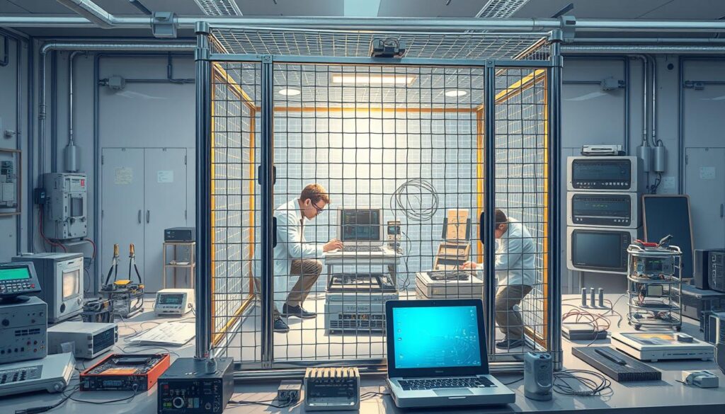
Faraday cages are a key tool. They block external electric fields, protecting sensitive electronics. Made from conductive materials like copper or aluminum, they enclose and shield what’s inside from outside fields.
Ground Plane Optimization
Designing a good ground plane is vital. It helps avoid ground loops and keeps signals clear. We use star or radial grounding to manage return currents. This keeps signals strong and reduces electromagnetic interference.
Power Distribution Network Design
A well-designed power network is key to EMI suppression. We use decoupling capacitors and ferrite beads to block noise. Capacitors fight high-frequency noise, and ferrite beads filter out unwanted interference.
With these techniques, we build a strong, reliable electrical system. It stands up to crosstalk and signal noise. This means our devices and systems work at their best.

Digital Signal Processing Methods for Noise Reduction
Digital signal processing (DSP) techniques are key to improving circuit performance. They help fight crosstalk and signal noise. Methods like adaptive filtering, equalization, and error correction are changing how we tackle noise in electronics.
Adaptive filtering is a crucial DSP technique. It adjusts its parameters based on the input signal. This makes it great for environments where noise changes over time.
Equalization is another important method. It shapes the frequency response to reduce noise. This is especially useful in high-speed data systems to keep signals clear.
Error correction algorithms also play a big role. They add redundancy to data to catch and fix errors. This ensures information gets through even when signals are poor.
These DSP techniques often use Field-Programmable Gate Arrays (FPGAs) and DSP hardware. These tools offer the power and flexibility needed for complex algorithms. They make noise reduction more effective.
Using these digital signal processing methods, engineers can better handle crosstalk and noise. This leads to better circuit performance and more reliable systems.

Testing and Measurement of Crosstalk and Signal Noise
In this section, we explore how to test and measure crosstalk and signal noise in electronic systems. We’ll look at oscilloscopes, spectrum analyzers, and network analyzers. These tools are key in this process. We’ll also talk about eye diagrams and S-parameters, which give us important insights into signal quality and system performance.
Oscilloscopes are crucial for analyzing crosstalk and signal noise. They let us see and measure the time-domain characteristics of electrical signals. By looking at waveforms, we can spot and measure unwanted signal interference like ringing and overshoot.
Spectrum analyzers help us understand the frequency-domain behavior of signals. They show us the spectral content and potential noise sources. This is important for identifying and fixing noise issues.
Network analyzers are also vital. They measure the frequency-dependent characteristics of circuits and connections. By analyzing S-parameters, we can understand signal integrity and find impedance mismatches that cause crosstalk and noise.

