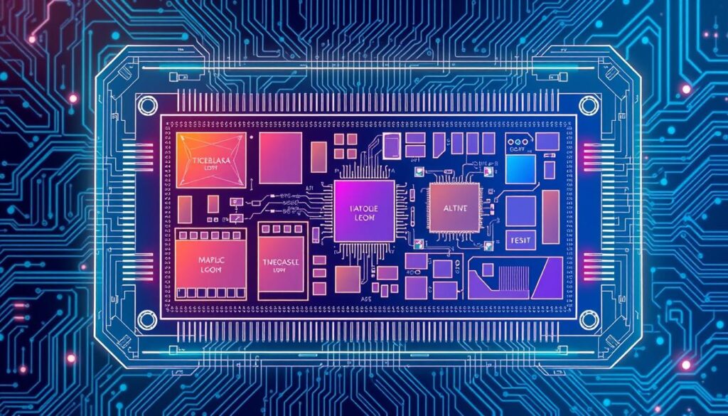
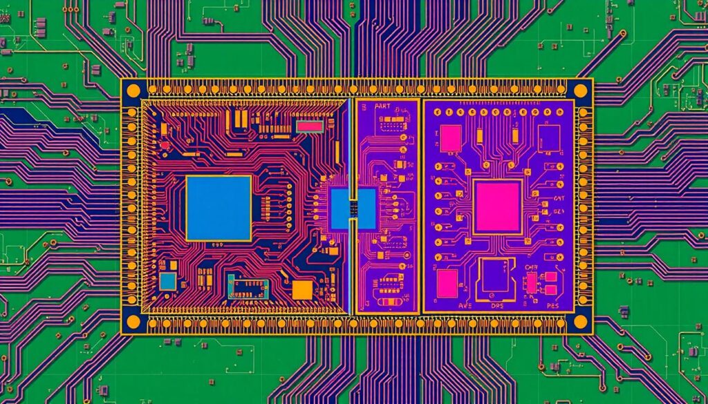
As an IC design professional, I know chip partitioning is key in floorplanning. It divides the chip into smaller blocks for easier handling. This step decides the floorplan’s size and shape, assigns blocks to designers, and looks at data flow.
Chip partitioning affects the design’s area, shape, and pin placement. While designers have some freedom, the floorplan’s quality greatly impacts the design’s Power, Performance, and Area (PPA).
Today, over 50 billion transistors fit in a single IC. The VLSI physical design flow has 8 steps, with chip partitioning being vital. It divides the chip into blocks for placement and routing, making design organization efficient.
Table of Contents
Understanding Floorplanning Fundamentals
Floorplanning is key in chip design, where we decide where everything goes. It’s about choosing the chip’s size and shape, where to put ports and pins, and more. This process starts with the chip’s design and goes through to the final stages.
Core Components of Floorplanning
The main parts of floorplanning are:
- Deciding the chip’s size and shape, with aspect ratio being important
- Where to put I/O ports and pins, which impacts how wires are laid out
- Placing macros, thinking about area, power, and timing
- Designing the power grid for efficient power delivery
- Putting standard cells in the best spots for performance
Design Flow Integration
Floorplanning fits right into the design process. It starts with the chip’s design and goes through to the end. The inputs include the chip’s netlist, design libraries, and technology files.
Initial Considerations and Requirements
At the start of floorplanning, we consider a few important things:
- Setting the core and die dimensions for chip area optimization
- Deciding where to put I/O pin placement around the chip’s edges
- Creating standard cell rows for efficient design flow and chip area optimization
- Handling wire length, routing, and IR drop issues for design performance
By focusing on these basics, floorplanning sets the stage for a successful chip design.
Chip Partitioning Strategies and Implementation
Chip partitioning is key to optimizing floorplans. It breaks down the design into blocks, each with its own tasks and connections. This approach helps use chip space better and improves the floorplan’s design.
Block-Level Division Techniques
Designers must think about several things when dividing the chip. They need to consider each block’s function, timing, and how they connect. By doing this, they can create a clear hierarchy that uses chip space well.
Partition Size Optimization
Getting the partition size right is important. It helps spread out the work among designers, making the design process smoother. Adjusting partition sizes ensures tasks are evenly distributed, avoiding delays.
Hierarchical Design Approaches
For complex chips, a hierarchical design is helpful. It breaks down the design into smaller parts, making it easier to manage. Tools help create and change the floorplan structure, exploring different layouts efficiently.
| Partitioning Strategy | Description | Advantages | Limitations |
|---|---|---|---|
| Spatial Data Partitioning (SDP) | Dividing the data across multiple chips based on spatial location | Reduced communication overhead, improved parallelism | Potential load imbalance, complex data management |
| Temporal Data Partitioning (TDP) | Dividing the data across multiple chips based on time sequence | Reduced latency, better utilization of chip resources | Increased communication overhead, synchronization challenges |
| Spatial Instruction Partitioning (SIP) | Dividing the instructions across multiple chips based on spatial location | Improved resource utilization, reduced communication | Potential load imbalance, complex control flow management |
| Temporal Instruction Partitioning (TIP) | Dividing the instructions across multiple chips based on time sequence | Better pipelining, reduced resource contention | Increased control overhead, synchronization issues |

Power Planning and Grid Design
Power planning and grid design are key in floorplanning. They involve designing the power structure and calculating stripe widths and distances. This is based on IR drop requirements and drawing power stripes in top metal layers. Initial power analysis checks IR drop and makes adjustments as needed.
In multi-voltage designs, creating voltage areas and placing isolation and level shifter cells is done. Power grid connections to all macros and preplaced cells are verified. The width and distance between stripes are calculated to meet IR drop requirements.
Designers aim for 65-75% area utilization in floorplanning. They choose more than one layer for I/O pins and keep enough space between them. This avoids routing design rule checks (DRCs). Floorplans with high utilization might face routing issues due to pin accessibility or congestion.
Partitioning blocks with similar power intent and clock domain simplifies low power design. Designers must carefully plan power routing to balance power drop and routing resources.
Designers aim for an even aspect ratio in floorplans for balanced routing. They avoid deep notches as they can harm timing, power, and area resources.
ESD clamp cells are added throughout the design to protect against external noise. Allocating space for routing feedthrough signals helps avoid congestion and signal crosstalk.
Macro Placement and Block Arrangement
In chip design, placing macros and blocks is key to top performance. Following macro placement rules is vital. It helps with efficient routing, solves power problems, and keeps the design solid.
Placement Guidelines for Optimal Performance
Macros should be placed near the core’s edge. This avoids routing blocks and reduces voltage drop issues. It also makes signal routing smoother, boosting system performance.
Channel Spacing Requirements
Spacing between macros is critical for good routing and power grid setup. The space needed depends on pin count and routing layers. Proper spacing ensures efficient use of resources and keeps the design reliable.
Handling Multi-Voltage Domains
Working with multiple voltage domains needs extra care. Designers must create voltage areas and use isolation cells for voltage level changes. Proper placement of macros and blocks is essential for smooth power flow and signal quality across domains.
Floorplanning tools use “flylines” to show and improve macro and I/O pin connections. “Halo regions” around fixed macros prevent other components from being too close. This helps avoid routing and timing problems.
| Floorplanning Metric | Optimal Guideline |
|---|---|
| Macro Placement | Place macros along core boundary to avoid routing obstructions and IR drop |
| Channel Spacing | Calculate spacing based on pin count and available routing layers |
| Multi-Voltage Domains | Create voltage areas and place isolation cells to manage voltage transitions |

Physical Constraints and Design Rules
In chip floorplanning, physical constraints and design rules are key. They guide the layout and placement of components. These rules help make the design feasible and efficient, focusing on placement blockages, routing constraints, and halo regions.
Placement blockages help control where standard cells go and reduce routing congestion. Hard blockages stop cell placement, while soft blockages allow buffer cells. Partial blockages help spread out components in certain areas, making space more efficient.
Halo regions, or keepout margins, keep macros safe from other design elements. This ensures there’s enough space for routing and avoids interference during implementation.
Design rules cover macro placement, channel spacing, and power grid design. Following these rules is crucial for a valid and efficient floorplan. It must meet performance and reliability goals.
| Constraint Type | Description |
|---|---|
| Placement Blockages |
|
| Halo Regions | Keepout margins around fixed macros to prevent nearby placement |
| Design Rules |
|
By using these physical constraints and design rules, floorplanning becomes more efficient. This leads to a strong and efficient chip layout that meets performance and reliability needs.
Conclusion
Floorplanning is key in making integrated circuits work well. It affects how chips perform, use space, and save power. A good floorplan helps with later steps like placing components and making the chip work smoothly.
Good floorplanning means dividing the chip well, placing important parts wisely, and managing power use. It also follows strict rules to ensure the chip works right.
Design teams now focus on chips that are part of bigger systems. Chips are getting more complex as they handle more tasks. This calls for chips with different parts for different jobs.
Working together, hardware and software teams make chips that use less energy but still perform well. This balance is crucial for chips to be efficient and powerful.
Improving the floorplan is vital for chips to work well and be easy to make. Tools like Methodics IPLM help by keeping everything organized. This makes designing chips more efficient.
By following best practices and using the latest design tools, teams can create top-notch floorplans. These meet the changing needs of the industry.
Source Links
- Steps In VLSI Physical Design Flow
- Partitioning In The Chiplet Era
- Floorplanning
- Introduction to Floorplan – VLSITutor
- A Transferable Approach for Partitioning Machine Learning Models on Multi-Chip-Modules
- VLSI: Physical Design (PD P1) — Introduction to PD
- The Ultimate Guide for Optimal SoC Floorplan – AnySilicon
- Custom Macro Placement
- Floorplanning: concept, challenges, and closure
- What is Partitioning in Physical Design ?
- Physical design (electronics)
- Partitioning For Better Performance And Power
- What Is Design Partitioning? | Perforce Software
- System partitioning in VLSI and its considerations

