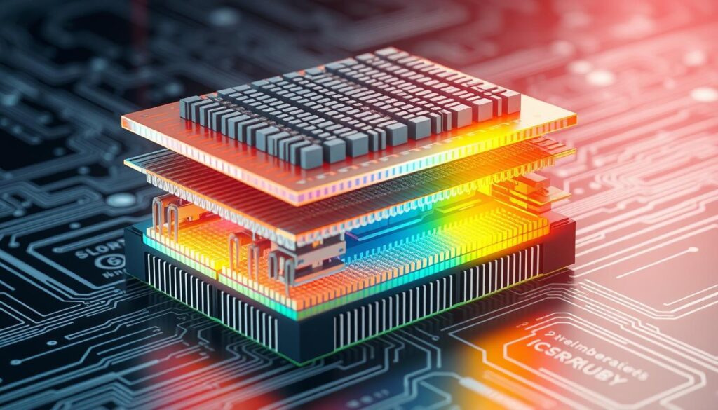
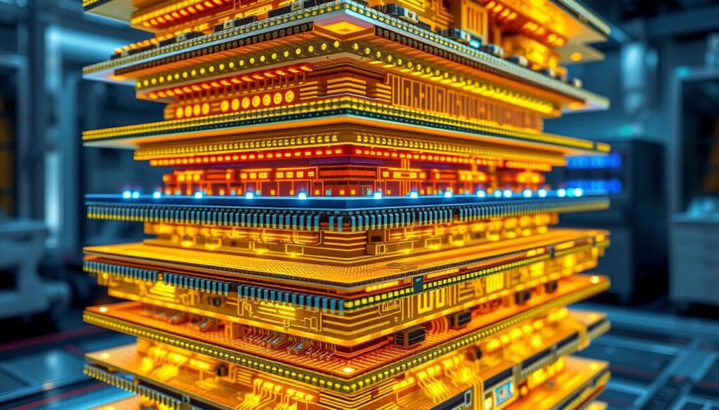
In the world of semiconductor technology, 3D integrated circuits (3D ICs) have brought new innovation and complexity. We face many challenges in 3D IC physical design. These include integrating Through-Silicon Vias (TSVs), managing heat, and optimizing power distribution.
The move from 2D chips to 3D structures has opened up new chances for better devices. We can now have more devices in less space, better performance, and save energy. But, this change also brings new design problems that need careful attention and a deep understanding of the technology.
In this article, we’ll look at the main challenges in 3D IC physical design. We’ll focus on TSVs, heat management, and power distribution. Our goal is to give a full view of the problems and solutions in modern chip design and manufacturing.
Table of Contents
Understanding the Fundamentals of 3D IC Physical Design
Exploring 3D integrated circuits (3D ICs) requires understanding their architecture and components. This technology is a big leap from traditional 2D circuits. It tackles Moore’s Law challenges, leading to better performance, power use, and size.
Basic Architecture and Components
At the heart of a 3D IC is chip stacking. This stacks multiple dies or layers vertically. It uses die-to-die interconnects for communication between layers. The components include dies, through-silicon vias (TSVs), and micro-bumps or solder balls for connections.
Evolution from 2D to 3D Integration
The shift to 3D integration is due to Moore’s Law scaling limits. 3D ICs offer a way to keep improving performance, power use, and size. They allow for more components in a smaller space and mix different technologies like logic, memory, and sensors.
Key Technology Drivers
Several factors drive 3D IC technology. Chip stacking and die-to-die interconnects improve performance, power use, and size. Heterogeneous integration also opens up new design possibilities, beyond what 2D integration can do.
Through-Silicon Via (TSV) Implementation Challenges
Creating Through-Silicon Vias (TSVs) in 3D integrated circuits (ICs) is tough. It involves many steps, from making the TSVs to how they affect the chip’s performance and reliability. Knowing these challenges is key to making 3D ICs work well.
The TSV making process is a big challenge. Designers face choices like via-first, via-middle, and via-last methods. Each has its own pros and cons. Things like TSV size, alignment, and how they fit into the process are important for success.
TSV capacitance and stress also matter a lot. TSVs can add unwanted capacitance, changing how the circuit works. This can affect signal quality and power use. Also, the stress from TSVs can cause problems like delamination and changes in device performance.
| TSV Fabrication Approach | Key Considerations |
|---|---|
| Via-first | High aspect ratio, process integration, yield |
| Via-middle | Alignment, process complexity, thermal management |
| Via-last | Interconnect performance, process integration, cost |
To tackle these issues, designers use advanced tools and techniques. They design TSVs in new ways and optimize the process. This helps make 3D ICs that are faster, use less power, and are more reliable.
Thermal Management and Heat Dissipation Issues
As 3D integrated circuits (ICs) get more advanced, managing heat becomes a big challenge. It’s important to handle thermal modeling, find effective cooling, and understand how heat affects performance. This ensures these high-tech chips work well and last long.
Thermal Modeling Complexities
Thermal modeling in 3D ICs is very complex. This is because of the vertical stacking of layers. The heat transfer between layers needs advanced simulation and analysis. We must look at hotspots, thermal coupling, and thermal vias to predict temperatures and find issues.
Cooling Solutions and Strategies
To tackle thermal issues in 3D ICs, many cooling solutions are being explored. Liquid cooling systems are showing great promise. They use special channels to remove heat. Also, thermal-aware design helps by placing heat sinks and optimizing heat paths.
Impact on Device Performance
Heat buildup in 3D ICs can harm performance, reliability, and lifespan. High temperatures cause leakage, slow speeds, and wear out devices faster. It’s key to solve these thermal problems to make 3D integration successful.
| Thermal Management Approach | Key Advantages | Potential Drawbacks |
|---|---|---|
| Liquid Cooling | Efficient heat dissipation, high thermal transfer rates | Increased complexity, potential for leaks, added power consumption |
| Thermal-Aware Design | Proactive heat management, optimized heat transfer paths | Requires detailed thermal modeling and analysis, potential design trade-offs |
| Advanced Heatsinks | Passive cooling, no additional power requirements | Limited heat dissipation capacity, potential for hotspot formation |
It’s vital to tackle thermal management and heat dissipation in 3D ICs to unlock their full potential. By using advanced thermal modeling, innovative cooling, and thermal-aware design, engineers can make sure these chips are reliable, perform well, and last long.

Power Distribution Network Optimization
Creating an efficient power distribution network is key in 3D Integrated Circuits (3D ICs). It helps keep power integrity and solve problems like voltage droop and IR drop. To optimize the power grid for 3D ICs, understanding the unique architecture and technology is crucial.
Voltage droop is a big concern in 3D IC power distribution. As devices get more integrated, keeping the voltage stable is harder. Decoupling capacitors help by storing energy and filtering out noise.
Managing IR drop is also vital. IR drop is the voltage difference due to power grid resistance. In 3D ICs, the network spans many layers, making IR drop worse. Using advanced design techniques can help reduce IR drop and keep power integrity.
Thermal effects on the power grid are also important. Heat can change the power grid’s resistance and capacitance, causing voltage issues. Good thermal modeling and cooling solutions are needed to handle these problems.
| Metric | 2D IC | 3D IC |
|---|---|---|
| Power Integrity | Moderate | High |
| Voltage Droop | Manageable | Challenging |
| IR Drop | Moderate | Significant |
| Decoupling Capacitor Placement | Simpler | Complex |
| Power Grid Design Techniques | Established | Evolving |
By tackling these challenges, designers can make 3D ICs work reliably and efficiently. This opens the door for more progress in this area.

Design for Testing and Verification Strategies
3D integrated circuits (3D ICs) bring new challenges that need strong design for test (DFT) and verification strategies. We face unique hurdles with this technology. These include pre-bond testing, post-bond testing, and the importance of known good die (KGD) testing.
Pre-bond Testing Methods
Before stacking and bonding, it’s crucial to test each die thoroughly. Advanced DFT techniques, like test access mechanisms (TAMs), help with this. They allow for die-level testing and fault model detection.
This early testing helps find and remove defective dies. It boosts the yield and performance of the final 3D IC stack.
Post-bond Testing Challenges
After the 3D IC stack is built, testing it is harder. The complex network of through-silicon vias (TSVs) and the system’s complexity are big challenges. New stack-level testing methods and updated fault models are key to maintaining quality.
They help find issues in the 3D structure.
Known Good Die Testing
The success of 3D ICs depends on known good die (KGD). This means each die in the stack must work perfectly. KGD testing, combining die-level and stack-level strategies, is vital.
It reduces yield loss and boosts the 3D IC’s reliability. Investing in KGD testing is crucial for 3D integration’s success.
The 3D IC world is growing, and so are the testing and verification challenges. Developing specific DFT, test access mechanisms, and fault models is key. These strategies will help us unlock 3D integration’s full potential.
They will lead to high-performance, energy-efficient, and compact integrated circuits.
Future Trends in 3D IC Physical Design
The future of 3D IC physical design is exciting. Monolithic 3D ICs are becoming more popular. They stack multiple layers of devices in one chip. This design boosts performance and saves energy by cutting down on connections and using silicon better.
Advanced packaging like system-in-package (SiP) and chiplet-based designs are also changing the game. These methods mix different components into one package. This includes analog, digital, and even neuromorphic computing blocks, making for a high-performance package.
3D ICs are also key to new computing ideas, like neuromorphic systems. They offer better connections and faster data flow. This could lead to big advances in machine learning and cognitive computing.

