Welcome to our article on SR Latch, an essential component in the world of digital circuits. Whether you’re an electronics enthusiast, an aspiring engineer, or simply curious about how digital devices work, understanding the SR latch is crucial.
An SR latch plays a vital role in data storage and logic functions within digital circuits. It enables electronic devices to retain and process information, making it a fundamental building block in various electronic applications.
In this comprehensive guide, we will dive into the intricacies of the SR latch, exploring its construction, operation modes, and timing considerations. Additionally, we will examine how it can be implemented using logic gates, ensuring a thorough understanding of its inner workings.
But first, let’s take a moment to grasp the importance of digital circuits in our daily lives. From smartphones to computers, digital devices surround us, reshaping the way we communicate, work, and entertain ourselves.
As we venture further into the article, you’ll gain valuable insights into the applications and use cases of the SR latch. Whether it’s memory storage, flip-flops, or finite-state machines, this versatile component proves to be a cornerstone in the world of digital circuit design.
So, buckle up and get ready to delve into the fascinating world of the SR latch and its role in creating innovative digital devices. Let’s unlock the potential of digital circuits together!
Table of Contents
Understanding the SR Latch
In this section, we will delve deeper into the workings of an SR latch. The SR latch is a bistable multivibrator, a circuit capable of storing and retaining data in two stable states: set and reset.
To understand the functioning of an SR latch, let’s explore its interactions between these two stable states:
Set State
When the SR latch is in the set state, the output is set to a high logic level (1) while the complementary output is set to a low logic level (0). This state is triggered by setting the S input to 1 while keeping the R input at 0.
Reset State
In contrast, when the SR latch is in the reset state, the output is set to a low logic level (0), and the complementary output is set to a high logic level (1). This state is triggered by setting the R input to 1 while keeping the S input at 0.
It’s important to note that if both the S and R inputs are set to 1 simultaneously, an invalid or indeterminate state may occur, making the latch unpredictable. To avoid this, it’s crucial to ensure proper timing and control of the inputs.
Now let’s visualize the set and reset states of an SR latch using a truth table:
| S | R | Q | Q̅ |
|---|---|---|---|
| 0 | 0 | Previous state | Previous state̅ |
| 0 | 1 | 0 | 1 |
| 1 | 0 | 1 | 0 |
| 1 | 1 | Indeterminate | Indeterminate |
This truth table illustrates the behavior of the SR latch depending on the inputs S and R. When S=R=0, the previous state is maintained. When S=0 and R=1, the latch enters the reset state with Q=0 and Q̅=1. Similarly, when S=1 and R=0, the latch enters the set state with Q=1 and Q̅=0. Finally, when both S and R are set to 1, the latch enters an indeterminate state, resulting in undefined outputs.
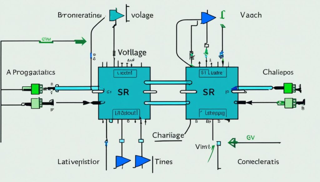
To better visualize the SR latch and its states, take a look at the following diagram:
Now that we have a clear understanding of the SR latch and its stable states, let’s explore its construction and implementation using logic gates in the next section.
Construction and Logic Gates Implementation
In this section, we will explore the construction of an SR latch and how it can be implemented using various logic gates, such as NAND or NOR gates. Understanding the construction of an SR latch is crucial for comprehending its inner workings and the role logic gates play in its operation.
The SR latch can be constructed using basic logic gates, providing a foundation for more complex digital circuit designs. The most common implementation of an SR latch involves using two cross-coupled NOR gates or NAND gates.
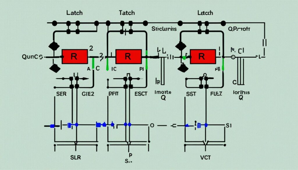
Let’s take a closer look at the construction of an SR latch using NOR gates:

The two NOR gates in an SR latch are connected in a feedback loop. This connection allows the latch to store and retain data, maintaining its state even when the inputs change. The set (S) and reset (R) inputs control the state of the latch, transitioning it from one stable state to another.
The truth table below illustrates the behavior of an SR latch:
SR Latch Truth Table
| S | R | Q | Q̅ |
|---|---|---|---|
| 0 | 0 | Previous state | Previous state complement |
| 0 | 1 | 0 | 1 |
| 1 | 0 | 1 | 0 |
| 1 | 1 | Not allowed | Not allowed |
The circuit diagram and the truth table provide insights into the behavior and functionality of an SR latch. By using logic gates, engineers can construct and customize SR latches to suit a wide range of digital circuit requirements.
Next, let’s explore how logic gates, such as NAND or NOR gates, can be utilized to implement an SR latch.
Operation Modes and Timing Considerations
When working with an SR latch, it is crucial to understand its different operation modes and consider the timing factors that can affect its performance. This section will explore the various operation modes of an SR latch, including the set, reset, hold, and not allowed states. Additionally, we will delve into the timing considerations, such as propagation delays and setup/hold times, that ensure accurate data storage and retrieval.
Operation Modes
The SR latch operates in different modes depending on the inputs it receives. Let’s take a closer look at each mode:
- Set State: In this mode, the “S” input is set to 1 while the “R” input remains at 0. This causes the latch to store a logic 1 at its output, also known as the Q state. The complement of Q, denoted as Q̅, will be 0.
- Reset State: Conversely, in the reset mode, the “S” input is set to 0 while the “R” input is set to 1. This results in the latch storing a logic 0 at its output (Q = 0, Q̅ = 1).
- Hold State: When both the “S” and “R” inputs are set to 0, the SR latch remains in its current state, holding the stored data.
- Not Allowed State: The not allowed state occurs when both the “S” and “R” inputs are set to 1 simultaneously. In this case, the behavior of the latch is undefined, and it may become unstable or oscillate between states.
Timing Considerations
Timing considerations play a crucial role in the proper operation of an SR latch. Two key timing parameters are propagation delay and setup/hold times:
- Propagation Delay: Propagation delay refers to the time it takes for a change in the inputs to propagate through the latch and be reflected at the outputs. It is important to consider the propagation delay to ensure that the stored data is stable and properly updated.
- Setup/Hold Times: The setup time is the minimum period before the clock edge where the inputs must be stable for the latch to capture the new data correctly. On the other hand, the hold time is the minimum period after the clock edge during which the inputs must be held stable for reliable data retention.
Ignoring proper timing considerations can result in data corruption and unpredictable behavior of the SR latch. Engineers must carefully analyze and design their circuits to meet the required timing specifications.
| Timing Considerations | Description |
|---|---|
| Propagation Delay | The time for a change in inputs to propagate through the latch |
| Setup Time | The minimum time before the clock edge for stable inputs |
| Hold Time | The minimum time after the clock edge for stable inputs |
Understanding the operation modes and timing considerations of an SR latch is essential for designing reliable and efficient digital circuits. By carefully considering these factors, engineers can ensure accurate data storage and retrieval, ultimately leading to successful circuit implementation.

Applications and Use Cases
The SR latch finds a wide range of applications in digital circuit design, playing a crucial role in various electronic systems. Let’s explore some of the key use cases where the SR latch proves to be invaluable:
1. Memory Storage
One of the primary applications of the SR latch is in memory storage. It can be used to store a single bit of data, representing either 0 or 1. The latch’s ability to retain the stored information even when the input signals are removed makes it ideal for temporary data storage in computer systems and microcontrollers.
2. Flip-Flops
The SR latch forms the basic building block of flip-flops, which are essential for sequential logic circuits. By combining multiple SR latches, more advanced flip-flop circuits like D flip-flops, JK flip-flops, and T flip-flops can be created. These flip-flops are widely used in shift registers, counters, and other circuits that require storing and manipulating binary information.
3. Finite-State Machines
In digital systems where the behavior and output depend on the current input and the previous state, finite-state machines (FSMs) are utilized. The SR latch, due to its bistable nature, can be employed to build the memory elements in FSMs. It enables the system to remember and transition between different states based on specific conditions, making it essential for designing control units, digital controllers, and complex state-based systems.
The applications of the SR latch extend beyond these examples, with its versatility and reliability making it a valuable component in numerous digital circuit designs.
| Application | Description |
|---|---|
| Memory Storage | Used to store a single bit of data in computer systems and microcontrollers. |
| Flip-Flops | The building block of various flip-flop circuits, enabling binary information storage and manipulation. |
| Finite-State Machines | Integral in creating memory elements for complex state-based systems and control units. |
By understanding the diverse applications and use cases of the SR latch, designers and engineers can harness its power to optimize digital circuit designs and achieve desired functionality.
Conclusion
In conclusion, the SR latch plays a fundamental role in the design of digital circuits. Its ability to store data and perform logic functions is critical in various electronic applications. By understanding the construction, operation modes, and timing considerations of the SR latch, engineers can effectively utilize this component to achieve desired outcomes in their designs.
The SR latch serves as a bistable multivibrator, capable of retaining data in its set and reset states. It can be constructed using logic gates such as NAND or NOR gates, allowing for flexible implementation in circuit designs. The latch’s different operation modes, including set, reset, hold, and not allowed states, provide engineers with the necessary flexibility to control data storage and retrieval.
Timing considerations, such as propagation delays and setup/hold times, are crucial in ensuring accurate data storage and reliable circuit operation. Engineers must take these factors into account when designing digital circuits that incorporate the SR latch. By doing so, they can optimize the performance and functionality of their designs.
Overall, the SR latch is an indispensable component in digital circuit design. Its versatility and functionality make it a key player in various electronic applications. Whether it’s used for memory storage, flip-flops, or finite-state machines, the SR latch provides engineers with the means to achieve efficient and reliable digital circuit designs.

