Welcome to our in-depth guide on the D Latch, an essential component in digital circuit design. In this article, we will explore the significance of D Latch in data storage and logic operations. Whether you’re a seasoned engineer or a budding designer, understanding the fundamentals of D Latch is crucial for creating efficient and reliable digital circuits.
The D Latch plays a pivotal role in digital circuit design, serving as a building block for various applications. Its primary function is to store information, allowing the circuit to retain a specific data value. This data storage capability is crucial when performing logic operations, enabling the manipulation of binary values to perform complex calculations and tasks.
In the realm of digital circuit design, the ability to store and manipulate data accurately and efficiently is paramount. With the D Latch, engineers and designers have a reliable tool at their disposal for creating robust digital circuits that can perform complex operations with precision. By leveraging the power of the D Latch, it becomes possible to construct systems that can process and transmit data effectively, paving the way for technological advancements across industries.
In the upcoming sections, we will dive deeper into the inner workings of the D Latch. We will discuss its structure, operation, construction techniques, timing characteristics, applications, and much more. By the end of this guide, you will have a comprehensive understanding of the D Latch and its role in digital circuit design.
Table of Contents
Understanding the D Latch
In this section, we will delve deeper into the D Latch to gain a comprehensive understanding of its structure and operation. A D Latch is a vital component in digital circuit design, specifically in the realm of latch circuits. We will explore the different variations of the D Latch, including the transparent latch, and examine the role of the latch enable signal in controlling the latch operation.
Latch Circuit and its Variations
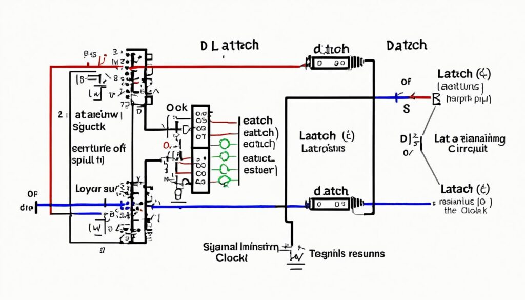
A latch circuit is a fundamental building block in digital electronics, used for temporarily storing data. The D Latch, in particular, allows for the transparent transfer of a single data bit from the data input (D) to the output (Q). It is known for its simplicity and efficiency in latch operations.
The transparent latch, also known as the gated D latch or data latch, is a variant of the D Latch that incorporates a latch enable input. This input signal, commonly referred to as the latch enable (LE) signal, controls the latch’s behavior by enabling or disabling the data transfer. When the latch enable signal is high, the D Latch is transparent, allowing the input data to propagate directly to the output.
If the latch enable signal is low, the D Latch is in the hold state, maintaining the previous output value irrespective of the input data. This characteristic makes the D Latch suitable for storing data during specific clock cycles or controlling the flow of information in sequential logic circuits.
Latch Operation and Timing
The operation of a D Latch depends on the state of its control signals, particularly the latch enable signal. When the latch enable is high, the D Latch operates in real-time, transparently reflecting any changes in the data input to the output. In contrast, when the latch enable is low, the D Latch remains in a hold state, preserving the output value.
To enable reliable latch operation, it’s crucial to consider timing characteristics such as setup time and hold time. Setup time refers to the minimum duration for which the D input must be stable before the rising edge of the latch enable signal, to ensure proper data storage. Hold time represents the minimum duration for which the D input must remain stable after the falling edge of the latch enable signal, to maintain data integrity.
D Latch Truth Table
| D input | LE input | Q output |
|---|---|---|
| 0 | 0 | Q(t-1) |
| 0 | 1 | 0 |
| 1 | 0 | Q(t-1) |
| 1 | 1 | 1 |
Table: D Latch truth table showcasing the correlation between D (data input), LE (latch enable), and Q (output) values. When LE is high, Q mirrors the D input in real-time, while it holds the previous output value when LE is low.
In the next section, we will explore the construction of a D Latch, shedding light on the use of cross-coupled NOR gates and the transistor-level implementation.
D Latch Construction
Constructing a D Latch involves utilizing cross-coupled NOR gates and implementing the design at the transistor level. By understanding the inner workings of these components, engineers can create efficient and reliable D Latches for various digital circuit applications.
Cross-Coupled NOR Gates
The core building blocks of a D Latch are the cross-coupled NOR gates. These gates are interconnected in a configuration that allows for feedback and latch functionality. The cross-coupling arrangement ensures that the output of one NOR gate affects the input of the other, creating a stable state for data storage.
The cross-coupled NOR gates operate based on the logical NOR function, where the output is high (1) only when both inputs are low (0). This behavior is crucial for the latch design, as it enables the storage of a single bit of information.
Transistor-Level Implementation
To implement a D Latch at the transistor level, engineers utilize complementary metal-oxide-semiconductor (CMOS) technology. CMOS offers low power consumption, high noise immunity, and excellent integration capabilities, making it ideal for digital circuit design.
The transistor-level implementation of a D Latch involves connecting multiple transistors according to the desired circuit design. MOSFETs (Metal-Oxide-Semiconductor Field-Effect Transistors) are commonly used in CMOS technology, providing the necessary control and switching functionality for the D Latch.
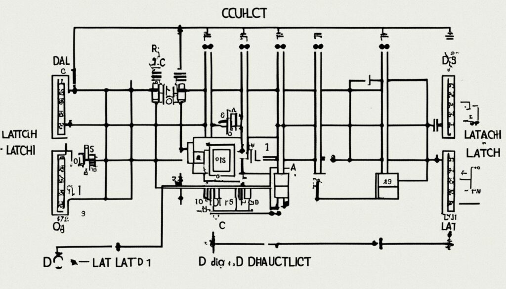
The image above illustrates a transistor-level implementation of a D Latch. The combination of cross-coupled NOR gates and MOSFETs enables data storage and the ability to control the latching behavior through appropriate input signals.
D Latch Timing and Signal Behavior
In digital circuit design, understanding the timing characteristics of a D Latch is crucial for ensuring reliable operation. Timing parameters such as setup time, hold time, and signal propagation play a significant role in the proper functioning of the latch.
Setup Time
Setup time refers to the minimum duration that the input signal must be stable before the clock edge. It ensures that the D Latch captures the correct data and avoids any timing violations. If the setup time is not met, the output may be unpredictable or erroneous.
Hold Time
Hold time is the minimum duration that the input signal must remain stable after the clock edge. It allows the D Latch to latch the data reliably and avoid potential signal distortion. Failure to meet the hold time requirement may result in metastability or incorrect output values.
Signal Propagation
Signal propagation refers to the time taken for an input change to propagate through the D Latch and reflect in the output. It determines the speed of data transfer and affects overall circuit performance. Minimizing signal propagation delays is crucial for high-speed digital systems.
By understanding and considering these timing characteristics, circuit designers can ensure the proper operation of D Latches in their designs, minimizing the risk of timing violations and optimizing circuit performance.

| Timing Characteristic | Description |
|---|---|
| Setup Time | The minimum time before the clock edge for stable input signal |
| Hold Time | The minimum time after the clock edge for stable input signal |
| Signal Propagation | The time taken for input change to propagate to the output |
D Latch Applications
In this section, we will explore the diverse range of applications for a D Latch in digital circuit design. The D Latch plays a crucial role in various areas, including data storage, flip-flops, memory elements, and sequential logic circuits.
Data Storage
One of the primary uses of a D Latch is in data storage. It provides a means to store and retain digital information in a circuit. The D Latch allows data to be latched and held until a new input is provided. This feature is essential in applications where temporary storage of data is required, such as data registers and memory buffers.
Flip-Flops and Memory Elements
Another significant application of a D Latch is in the construction of flip-flops and other memory elements. Flip-flops are widely used in digital systems for their ability to store and control data in sequential circuits. By combining multiple D Latches, flip-flops can be created to store binary information and facilitate clocked operations. These memory elements are integral for tasks such as data synchronization, state storage, and control signal generation.
Sequential Logic Circuits
Sequential logic circuits, including counters, shift registers, and finite-state machines, heavily rely on D Latches. These circuits require memory elements to store and manipulate data in a sequential manner, and the D Latch serves as a building block for implementing these functionalities. By incorporating D Latches into sequential logic circuits, designers can create complex systems that perform various tasks based on past and current inputs.

| Application | Description |
|---|---|
| Data Storage | Allows temporary storage of data in registers and buffers. |
| Flip-Flops | Enables the creation of memory elements for sequential circuit design. |
| Sequential Logic Circuits | Facilitates the implementation of counters, shift registers, and finite-state machines. |
Conclusion
In conclusion, the D Latch is a fundamental building block in digital circuit design. Its importance lies in its ability to store and manipulate data, making it an essential component in various applications.
Throughout this article, we explored the structure, operation, construction, timing characteristics, and applications of the D Latch. By understanding the fundamentals of this circuit, engineers and designers can enhance their knowledge and skills in creating efficient and reliable digital circuits.
The D Latch’s versatility allows it to be employed in various scenarios, from data storage to the creation of flip-flops and sequential logic circuits. Its use as a latch enables controlled data storage and facilitates complex logic operations.
By mastering the functionality and applications of the D Latch, designers and engineers can achieve optimal performance and reliability in their digital circuit designs, contributing to the advancement of technology across various domains.

