

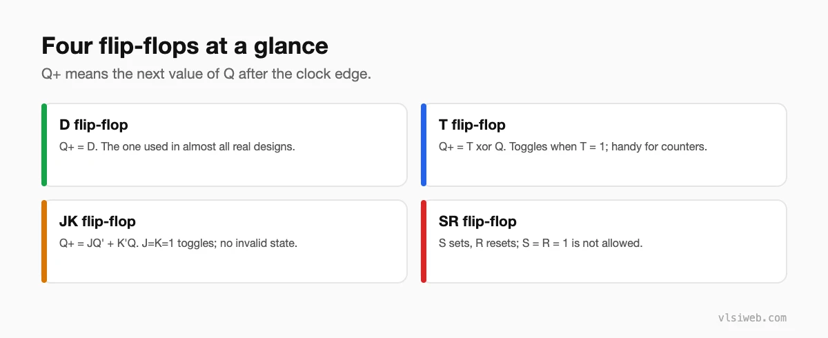
The short answer: a flip-flop stores one bit and updates only at a clock edge. The D flip-flop (Q+ = D) is the one used in almost all real designs. The T flip-flop toggles when T = 1, the JK flip-flop sets, resets or toggles depending on J and K, and the SR flip-flop sets or resets but forbids S = R = 1. Any of them can be built from a D flip-flop and a little logic.
This post combines my older posts on D, JK, T and SR flip-flops and clocking in flip-flops.
- Four flip-flops at a glance
- Characteristic tables
- The D flip-flop in Verilog
- Edge triggering and the master-slave structure
- Why D flip-flops won
Table of Contents
Part 1: Four flip-flops at a glance
Part 2: Characteristic tables
| J | K | Q+ |
|---|---|---|
| 0 | 0 | Q (hold) |
| 0 | 1 | 0 (reset) |
| 1 | 0 | 1 (set) |
| 1 | 1 | Q’ (toggle) |
| T | Q+ |
|---|---|
| 0 | Q (hold) |
| 1 | Q’ (toggle) |
Part 3: The D flip-flop in Verilog
module dff (
  input  wire clk, rst_n, d,
  output reg  q
);
  always @(posedge clk or negedge rst_n)
    if (!rst_n) q <= 1'b0;
    else        q <= d;
endmodule

// T flip-flop built from a D flip-flop
always @(posedge clk or negedge rst_n)
  if (!rst_n) q <= 1'b0;
  else        q <= q ^ t;
Part 4: Edge triggering and the master-slave structure
A positive-edge D flip-flop is two latches in series: a master latch that is transparent while the clock is low, and a slave latch that is transparent while it is high. At the rising edge the master closes and the slave passes its value to Q, so the output changes only at that edge. Some libraries also offer negative-edge flops, which sample on the falling edge.
Part 5: Why D flip-flops won
Standard-cell libraries are built around D flip-flops (often with scan, enable or reset variants). JK, T and SR behaviour is easy to build from a D flop and some logic, and having one kind of storage element makes timing analysis, DFT scan insertion and physical design much simpler.
Practise this on VLSI Forge
I built VLSI Forge so you can write RTL in your browser, run it on a real simulator and check every signal in the waveform. Free, nothing to install.
Flip-flop and counter problems
FAQ
Which flip-flop is used most in real chips?
The D flip-flop, usually with variants for reset, enable and scan.
Why does the JK flip-flop not have an invalid state?
Because J = K = 1 is defined as toggle, unlike S = R = 1 in an SR flip-flop.
What is clock-to-Q delay?
The time from the active clock edge to the output changing. It is part of every timing path.
Can a T flip-flop divide a clock by two?
Yes. With T = 1 it toggles every edge, giving an output at half the clock frequency.
