
The semiconductor industry lies at the heart of modern technological advancement. From powering smartphones to enabling complex artificial intelligence computations, semiconductors drive innovation. However, this intricate domain faces various challenges, from manufacturing intricacies to ensuring optimal performance and reliability.
Among the most prominent issues are defect identification, electrical performance, and fault isolation in increasingly compact designs. Advanced diagnostic tools like Electron Beam Absorbed Current (EBAC) have emerged as transformative solutions to address these challenges.
Understanding the Semiconductor Landscape:
Semiconductors are meticulously crafted from silicon and other materials to control electrical currents. As device functionalities increase, manufacturers push for smaller, faster, and more efficient designs. While this miniaturization is groundbreaking, it also introduces a higher susceptibility to faults, reduced yields, and increased production costs.
Table of Contents
Challenges in Semiconductor Development
1. Scaling Complexity
Modern semiconductor devices are now being developed with process nodes as small as 3 nanometers. This scaling reduces the available area for circuitry, making components highly sensitive to defects. Even a minute flaw can disrupt functionality and lead to performance degradation or complete device failure.
2. Fault Detection and Isolation
The presence of electrical shorts, open circuits, and high-resistance paths in tiny interconnects can severely hinder semiconductor performance. Traditional fault analysis techniques often struggle to accurately pinpoint these issues, especially in advanced nodes.
3. Performance Optimization
Performance optimization demands in-depth insights into current flow and electrical properties across the device. Engineers require detailed knowledge of how electrical signals travel through increasingly complex circuitry to enhance efficiency.
EBAC: A Transformative Diagnostic Tool
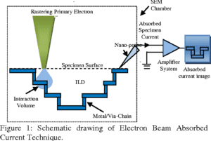
Electron Beam Absorbed Current (EBAC) is a non-invasive, high-resolution technique employed to analyze electrical current paths in semiconductor devices. This method uses a finely focused electron beam to induce currents, which are then measured to reveal electrical anomalies and performance bottlenecks.
How EBAC Works
- Electron Beam Interaction: An electron beam is directed onto the semiconductor’s surface, interacting with the material and generating electron-hole pairs.
- Current Measurement: These pairs create currents, which are absorbed by electrodes connected to the device under test.
- Signal Analysis: The absorbed current is measured to provide a detailed electrical map of the circuit. Variations in the current indicate potential issues like resistive paths, open circuits, or shorts.
Applications of EBAC
- Defect Localization: Identifying the exact location of shorts and opens in metal interconnects.
- Resistance Mapping: Measuring resistance in nanoscale features to detect anomalies.
- Failure Analysis: Providing insights into component degradation or manufacturing defects.
- Process Validation: Ensuring compliance with manufacturing standards and process reliability.
Key Benefits of EBAC in Semiconductor Diagnostics
Precision and Accuracy:
EBAC delivers unmatched precision in detecting electrical anomalies, even in the most intricate semiconductor architectures. Its ability to localize faults within nanometers makes it indispensable for advanced technology nodes.
Non-Destructive Analysis:
Unlike destructive techniques that compromise the device’s integrity, EBAC preserves the sample, enabling further testing and verification.
Enhanced Visualization:
EBAC solutions offer high-resolution current maps, providing engineers with actionable insights into electrical behavior and precise fault locations.
Role of Third-Party Laboratories
As semiconductor complexity grows, manufacturers increasingly turn to third-party laboratories for advanced diagnostics and testing. Wintech Nano, a leading third-party laboratory in Singapore, has established itself as a trusted partner for semiconductor analysis.
The lab’s expertise in cutting-edge diagnostic tools, including EBAC, enables manufacturers to overcome challenges in defect detection and performance enhancement efficiently. By combining state-of-the-art technology with a commitment to excellence, the laboratory helps clients achieve unparalleled product reliability and performance.
EBAC in Action: Real-World Applications
Addressing Yield Issues in Advanced Nodes:
A semiconductor manufacturer encountered significant yield losses due to defects in its 5nm production line. Using EBAC, engineers traced the defects to high-resistance paths in interconnects caused by process irregularities. By identifying and rectifying the issue, the company improved its yield by 15%.
Enhancing Device Reliability:
A consumer electronics company sought to improve the reliability of its microprocessors. EBAC analysis revealed latent defects in critical circuitry, which were subsequently mitigated through design modifications. This intervention resulted in a 20% reduction in failure rates during field testing.
Future of EBAC in the Semiconductor Industry
As semiconductor devices continue to evolve, EBAC is poised to play an even more critical role in ensuring performance and reliability. With advancements in electron beam technologies and data analysis algorithms, EBAC is expected to offer faster, more detailed, and more actionable insights.
Integration with AI:
AI-powered data processing could significantly enhance EBAC’s diagnostic capabilities, enabling real-time defect detection and predictive maintenance.
Wider Adoption:
As industry awareness grows, more manufacturers are likely to incorporate EBAC into their standard diagnostic processes, further driving innovation and reliability.
How Premier Laboratories Are Leading the Way in Navigating Semiconductor Challenges?
Premier 3rd party laboratories are leading the way in exemplifying the integration of advanced diagnostic techniques with industry expertise. Their use of EBAC, along with other state-of-the-art technologies, empowers semiconductor manufacturers to navigate challenges effectively. Through meticulous analysis and tailored solutions, the lab ensures that clients can consistently deliver high-quality, reliable products.
Conclusion
Navigating the complexities of semiconductor development requires sophisticated tools and expertise. EBAC has proven to be a game-changer in addressing the industry’s most pressing challenges, offering precision, reliability, and actionable insights. With the support of leading laboratories, manufacturers can confidently innovate, ensuring the continued advancement of semiconductor technologies that power our modern world.