

The short answer: VLSI grew out of the transistor (1947) and the integrated circuit (late 1950s). The first commercial microprocessor arrived in 1971, and the 1980s brought the VLSI era proper: hardware description languages, logic synthesis and automated design tools. The fabless and foundry model followed, then decades of scaling to billions of transistors, and today the industry is moving to gate-all-around transistors, chiplets and AI accelerators.
The old version of this page was a 5,000-word essay. History is interesting, but most readers want the main turning points and why they matter today. So here is the short version, focused on what still shapes how chips are designed.
- The milestones at a glance
- From transistor to integrated circuit
- Microprocessors and Moore’s law
- The VLSI era and design automation
- Fabless companies and foundries
- Where we are now
Table of Contents
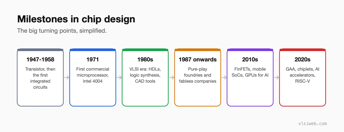
Part 1: The milestones at a glance
Part 2: From transistor to integrated circuit
The transistor was invented at Bell Labs in 1947. In 1958 and 1959, Jack Kilby at Texas Instruments and Robert Noyce at Fairchild independently built the first integrated circuits, putting several components on one piece of semiconductor. That idea, many devices on one chip, is the foundation of everything since.
Part 3: Microprocessors and Moore’s law
In 1965 Gordon Moore observed that the number of components on a chip was doubling regularly, which became known as Moore’s law. In 1971 Intel released the 4004, the first commercial microprocessor, with about 2,300 transistors. Modern chips have tens of billions.
Part 4: The VLSI era and design automation
By the late 1970s and 1980s chips were too large to draw by hand. Carver Mead and Lynn Conway’s work made VLSI design teachable and systematic, hardware description languages like Verilog and VHDL appeared, and logic synthesis turned code into gates automatically. This is when the modern design flow, and the EDA industry, really took shape.
Part 5: Fabless companies and foundries
In 1987 TSMC was founded as a pure-play foundry, making chips designed by other companies. This made the fabless model possible: companies that only design chips. It is why so much chip design today happens in design centres around the world, including India, separate from where the chips are manufactured.
Part 6: Where we are now
Scaling continued through planar transistors to FinFETs in the 2010s and now to gate-all-around transistors. At the same time, the industry is turning to chiplets and advanced packaging, specialised AI accelerators and open architectures like RISC-V. I cover these in more detail in VLSI industry trends that matter now.
Practise this on VLSI Forge
I built VLSI Forge so you can write RTL in your browser, run it on a real simulator and check every signal in the waveform. Free, nothing to install.
FAQ
What does VLSI stand for?
Very Large Scale Integration: putting a very large number of transistors on a single chip.
Who invented the integrated circuit?
Jack Kilby at Texas Instruments and Robert Noyce at Fairchild Semiconductor, independently, in 1958 and 1959.
Is Moore’s law dead?
Transistor density still increases, but more slowly and at much higher cost. Much of the progress now comes from packaging, chiplets and specialised designs.
When did India start doing chip design?
Major global companies began setting up design centres in India from the 1980s onwards, and India is now one of the world’s largest chip design hubs.
